


How to Use Ansible for Automated Server Setup

Ansible 101: Install, Configure, and Automate Linux in Minutes

10 Bash Scripts to Automate Daily Linux SysAdmin Tasks

Windows Subsystem for Linux is now Open Source

Tails OS Tutorial | Features, Installation, Pros, Cons

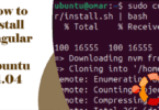
Ubuntu 25.04 Plucky Puffin – A Brief Walkthrough

awk Command in Linux

12 Best Linux Browsers in 2025

10 Best Linux Distros in 2025
How to Change Your Prompt in Bash Shell in Ubuntu

How to Install Steam on Ubuntu 24.04

How to Configure Proxmox VE 8 for PCI/PCIE and NVIDIA GPU Passthrough

How to Install VirtualBox on Ubuntu 24.04

Important Proxmox VE 8 PCI/PCIE Passthrough Tweaks, Fixes, and Workarounds

How to Install Proxmox VE 8 on Your Server

How to Upload/Download ISO Images on Proxmox VE Server

How to Keep Proxmox VE 8 Server Up-to-date

How to Enable SR-IOV from the BIOS/UEFI Firmware of Your Motherboard

How to Enable IOMMU/VT-d from the BIOS/UEFI Firmware of Your Motherboard

How to Create a Bootable USB Thumb Drive of Proxmox VE 8

How to Configure FirstUseAuthenticator on JupyterHub

Install MySQL on Ubuntu 24.04

6 Ways of Opening the Task Manager app on Windows 10/11

Install Conda on Ubuntu 24.04

Install Java on Ubuntu 24.04

Install NPM on Ubuntu 24.04

How To Use Grep Command in Linux

How to Change File Permissions in Linux

How To Use Traceroute Command in Linux

How To Use htop Command in Linux

How To Delete a File in Linux

How To Set Logrotate on Linux

How To Set up a Cron Job in Linux

How to List Processes in Linux

Best Linux Remote Desktop in 2024

Install Git on Ubuntu 24.04

How To Find a File in Linux

How to Unzip Files in Linux

How to Install QEMU Guest Agent on Proxmox VE Linux Virtual Machines

How to Enable QEMU Guest Agent on a Proxmox VE Virtual Machine

How To Create a User in Linux

How To Delete a Directory in Linux

How To Create a Tarball in Linux

Install vscode on Ubuntu 24.04

How To Use Rufus in Linux

How To Use the wget Command in Linux

How to Install VirtIO Drivers and QEMU Guest Agent on Windows 10/11 Proxmox VE Virtual Machines
How to Install pip on Ubuntu 24.04

How To Use the Reboot Command in Linux

How To Use the history Command in Linux

How To Use the Rsync Command in Linux

Install deb File on Ubuntu 24.04

How To Set Environment Variables in Linux

How to Clear Screen in Linux

What is a Filesystem in Linux

How To Create a File in Linux

How to Add a User to a Group in Linux

How To Install Anaconda on Linux

How to Zip Files in Linux

How To Use dig Command in Linux

How To Use alias Command in Linux

What Is Apt in Linux

How To Use Screen Recorder in Linux

How To Use Cat Command in Linux

How to Use YUM in Linux

How To Kill a Process in Linux

How to Use sudo in Linux

How To Use Chown Command in Linux

How To Check Load Average on Linux

How To Create a Directory in Linux

Best Arch Linux Based Distros of 2024

Best Linux Desktop Environment In 2024

How to Import a VMware Virtual Machine to Proxmox VE 8
How to check which Ubuntu Version you are on

Basic Vim Editor Commands

Install Docker on Ubuntu 24.04

How to Mount a USB Thumb Drive, HDD, or SSD on Proxmox VE

How to Install Google Chrome on Ubuntu 24.04

How to Add a Windows SMB/CIFS Share as Storage on Proxmox VE

goto Statement in C

How to Export VMware Workstation Pro Virtual Machines in OVF/OVA Format

How to Install the Official NVIDIA GPU Drivers on Proxmox VE 8

How to Generate LetsEncrypt SSL Certificate using CloudFlare DNS-01 Challenge and Use it on Synology NAS

How to Find the Chipset Driver/Firmware to Install to Get WiFi/Ethernet Devices to Work on Linux

Add a Column to the Table in SQL

How to Install Redis CLI on Linux

How to Access Proxmox VE Virtual Machines and LXC Containers Remotely via SPICE Protocol using Virt-Viewer

Emacs Key Bindings

Highlight the Current Line in Emacs

Select All Text in Emacs

Reload the Current File in Emacs
Compare Two Tables in SQL

Combine Two Columns in SQL

Simple and Advanced Alias Command Examples and Explanation

Python Tkinter Examples

Increase Font Size in Emacs on Linux
How to Install Angular on Ubuntu 24.04

How to Create Multiple NetworkManager Connection Profiles for the Same Network Interface on Linux and Switch Between Them

How to Install Podman on Ubuntu 24.04

Method to Install and Run OneNote Note-Taking App on Ubuntu 24.04

How to Enable/Disable WiFi Devices from the Command-Line on Linux Using NetworkManager

How to Implement Effective Health Checks in HAProxy

SQL Having Clause

SQL Subtract

SQL Select All Except

SQL Outer Join

Case Insensitive SQL LIKE Operator

SQL Lead Function
SQL Lag

How to Connect to WiFi Network from the Command-Line on Linux Using NetworkManager
Emacs Close Buffer

SQL Having Count Clause

Get the Month from a Given Date in SQL

Delete a Row in SQL

SQL COUNT WHERE

How to Use Lisp in Emacs

How to Use Emacs Themes

How to Use Emacs Org Mode

How to Update Parrot OS

How to Set Up a Static IP Address on WiFi Network from the Command-Line on Linux using NetworkManager

How to Install the Correct Chipset Driver/Firmware for WiFi/Ethernet Devices to Work on Fedora 39+

How to Run Kali Linux on Docker?
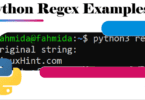
Python Regex Examples

Add Days to Date in SQL

Service vs. Systemctl
Restart a Service using systemctl restart Command

Restart Network Service using systemctl Command

Mount Windows Share on Linux using CIFS

How to Use the DS3231 Real-Time Clock (RTC) Module with an ESP32

Mount Windows NTFS Drive on Linux

Linux systemctl reboot Command

How to View Systemctl Logs

Linux Commands to Check Disk Partitions

How to Use Hashcat in Kali Linux?

How to Switch Boot Targets with systemctl Command

How to Use systemctl status Command

How to Use systemctl to Show Failed Units

How to Use systemctl Command to Enable and Disable Services

How to Set up and Program the ESP32 to Communicate with an Android Smartphone via Bluetooth

How to Start Docker Using systemctl Command

How to Mask a Service using systemctl Command

How to List Serial Ports on Linux

Systemd Service File

SQL StartsWith() Operator

Select the Top 10 Rows in SQL

Select the Most Recent Record by Date in SQL

Select Count Distinct in SQL

SQL SELECT AS

SQL Percentile

SQL PARTITION BY Clause

Merge Two Tables in SQL

SQL Limit

SQL FOR XML PATH

Join Three Tables in SQL

SQL DROP TABLE Statement
SQL DENSE_RANK() Function

SQL Distinct

Delete a Table in SQL

Count Rows in SQL
Count Duplicates in SQL

SQL Coalesce Null Values

SQL Ascending Order

How to Get Let’s Encrypt SSL Certificates Using Certbot CloudFlare DNS Validation

How to Enable EPEL Repository on RHEL 9/AlmaLinux 9/Rocky Linux 9/CentOS Stream 9

How to Interface MicroSD Card Module with ESP32 Using Arduino IDE

How to Fix systemctl status Showing Degraded State

How to Access Kali Desktop Using Remote Desktop Protocol

How to Delete a Systemd Service File

How to Create and Manage User Services on Linux

How to Create a Service File in Linux
How to Clear Swap on Linux

Git “Tip of Your Current Branch Is Behind” Error

Git “Support for Password Authentication Was Removed” Error

Git “Pre-Receive Hook Declined” Error

Git “Use a Personal Access Token Instead” Error

Arduino Nano Every Pinout

Delete a Fork in Git

Git Clone “Support for Password Authentication Was Removed” Error

How to Install Resolvconf on Debian 12

SQL “Is Not Null” Operator

SQL String Formatting

Add Months in SQL

Return Reference in C++

MySQL INSERT IGNORE Clause

How to Use the Cat Command to Write a Text to a File

How to Secure Your HAProxy with SSL

How to Find Syslog Location in Linux

“Pull Is Not Possible Because You Have Unmerged Files” Error in Git

Ignore the Package-Lock.JSON File in Git

Git Clone Exit Status 128

Git Clean Flags

Git “Cannot Publish Unborn Head” Error

Change the Table Name in SQL

Cast Various Types into an Int Data Type in SQL

Cast Various Types into Decimal Types in SQL

SQL Absolute Value
SQL Backup Table

How to Install the Latest NextCloud AIO (All In One) on Ubuntu/Debian/Fedora/RHEL/AlmaLinux/Rocky Linux/CentOS Stream

Python Subprocess.Popen Examples

Linux Logrotate Examples

Python String Examples

How to Set Up HAProxy with Keepalived for High Availability

How to Enable VirtIO-GL/VirGL 3D Acceleration on Proxmox VE 8 Virtual Machines

How to Implement SSL Passthrough in HAProxy

How to Install HAProxy on Debian Linux

How to Handle UDP Traffic with HAProxy

How to Add/Remove Kernel Boot Parameters/Arguments and GRUB Boot Entries on Fedora/RHEL/AlmaLinux/Rocky Linux/CentOS Stream

How to Configure HAProxy for WebSocket Connections

How to Add and Enable Proxmox Community Package Repositories on Proxmox VE 8 Server

“Src Refspec Does Not Match Any” Error in Git

Frozen Git Push

SQL RTRIM()

“Unable to Update a Local Ref” Error in Git

SQL XOR Operator

SQL WITH Clause

Replace a String in SQL

SQL REGEXP_REPLACE

List the Tables in SQL

List the Databases in SQL

Insert the Date Values in SQL

SQL Identity Columns

Get the Current Date in SQL

SQL First Day of the Month

SQL DATE_TRUNC

SQL CURRENT_DATE

SQL String Contains

SQL Comment

Check If the Column Exists in SQL

ESP32 Real Time Clock (RTC) Using DS1307 and OLED Display

ESP32 Web Server Using Arduino IDE

SQL Fetch

Divide Two Columns in SQL

SQL Cumulative Sum

“Git: Host Key Verification Failed” Error

Ignore the Env Files in Git

How to Check Kernel Version in Linux

How to Count the Number of Files in a Directory on Linux

How to Export the Ld_Library_Path in Linux

Size_t in C++

Socket Programming in C++

Examples of the Curl Get Command

SQL “Using” Query

SQL Min() Function

Multiply Two Columns in SQL

SQL Multiply

SQL Parameterized Query

Remove the Leading Zeroes in SQL

Remove Spaces in SQL

SQL Round Down

Create a Function in SQL

SQL Scope_Identity

Copy a Table in SQL

Convert INT to String in SQL

“SQL Command Not Properly Ended” Error

SQL SHOW TABLES

SQL String Aggregate Functions
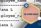
SQL String Equals

SQL WHERE IN Clause

What Is Let’s Encrypt DNS-01 Challenge and How to Use It to Get SSL Certificates?

Rootless Installation of Kali Linux in Termux

Zsh Vim Mode

VirtualBox vs Hyper-V vs VMware | Detailed Comparison

Vim Keyboard Shortcuts and Commands

How to pass through a USB in VirtualBox?

Stream Editor (SED): The Basics

How to Capture and Analyze the Packets by Example with Tcpdump

HAProxy Beginner’s Tutorial

How to Configure HAProxy as a Reverse Proxy

How to Set Up and Understand Logging in HAProxy
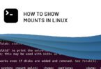
How to Show Mounts in Linux
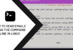
How to Send Emails Using the Command Line in Linux
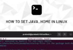
How to Set JAVA_HOME in Linux

How to Search File Contents in Linux

Isnumber in C++

Install Kali Linux on Android

Install Kali Linux on VMware

Linux cifs Mount

Login As Root on Ubuntu

How to Update Kali Linux?

How to Set Up Kali on WSL

How to Secure Kali Linux

Install Helm on Ubuntu

How to Reset Kali’s Forgotten Password?

How to Install Windows 11(Virtual Machine) on VMware?

How to Install Windows 11(Virtual Machine) on VirtualBox?

How to Install KDE Plasma Desktop on Kali Linux

How to Install Windows 7(Virtual Machine) in VMware?

How to Install Windows 7(Virtual Machine) in VirtualBox?

How to Install Windows 10(Virtual Machine) in VMware?

How to Install Windows 10(Virtual Machine) in VirtualBox?

How to install VirtualBox Guest Addition Image in a Virtual Machine?

How to Fix the “VirtualBox Drag and Drop not Working” Issue?

Fix the “Update && Upgrade” Command Error in Kali Linux on Android

Fix “NetworkManager is Not Running” on Kali Linux

Creating and Running a Linux “.a” File

CharAt() in C++

Best Linux Distributions in 2024

Bash Cut Examples

Automount Drives on Linux