What is Bipolar NPN Transistor
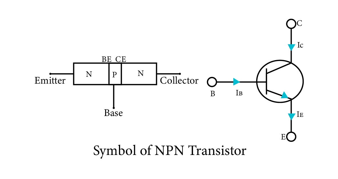
The bipolar junction transistor has mainly two types that are NPN and PNP transistors. In the NPN transistor, there is one P-type semiconductor material placed in the middle of two N-type semiconductor materials. The PNP transistor is opposite to it.
Configuration of NPN Transistor
The three terminals and two junctions of NPN transistor concerning semiconductor materials are:
Terminals
- Emitter (N-type material – Heavily Doped)
- Base (P-type material – Lightly Doped)
- Collector (N-type material – Moderately Doped)
Junctions
- Base-Emitter Junction
- Collector-Base Junction
The base of the NPN transistor is lightly doped to allow the least recombination in the base region. In an NPN transistor, the base is a source of current, and current is amplified through the NPN transistor, and a large current is obtained at the collector.
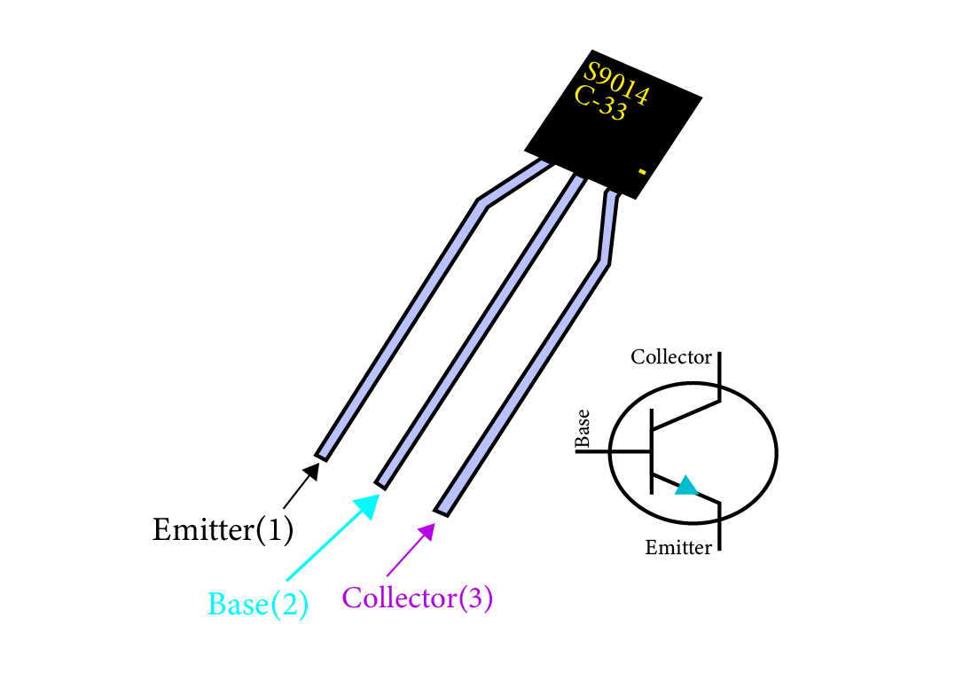
NPN Transistor looks as shown below:
Pinout Diagram of NPN Transistor
While facing the plane side of the transistor, the leftmost pin is the emitter terminal, the middle pin is the base terminal, and the rightmost pin represents the collector terminal. The Pinout of the NPN transistor is given below.
How Does an NPN Transistor Work
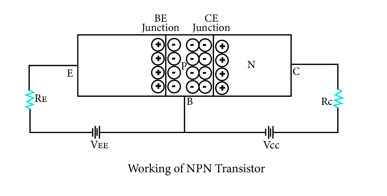
The base-emitter junction is forward-biased through VEE whereas the base-collector junction is reverse-biased through VCC.
The depletion region of the base-emitter junction is thin, whereas the base-collector junction’s depletion region is thick due to reverse-biased conditions. When VEE is applied, electrons start moving from N-type material towards P-type material, and due to the movement of electrons, a current start to flow through the emitter-base junction. This current is called emitter current, denoted by IE.
These electrons drift towards the base; however, the base is lightly doped, so a small amount of them merge with holes in the base, and the remaining move towards the collector.
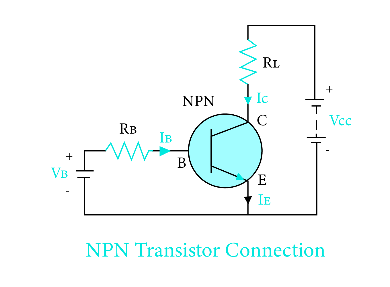
A small current known as IB flows through the base as electrons combine with holes. The electrons that go towards the collector region form collector current, represented as IC. The collector current is large as compared to the base current. The sum of both base and collector current constitutes emitter current.
The formula to calculate the base and collector current from the circuit is given below:
The relationship between IC and IB is given through ß:
Where ß is the current gain obtained through amplification.
Operating Modes of NPN Transistor
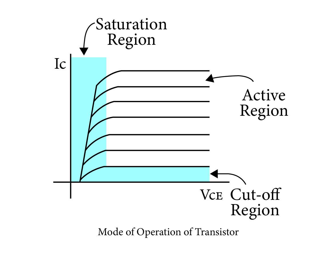
The modes of operation are decided through biasing of junctions. There are three modes of operation of NPN transistors.
1. Active Mode of Operation
In this mode, the emitter-base junction allows current in the forward direction, and the base-collector junction does not allow current to flow as it is reverse-biased. A large number of holes transfer current starting from the emitter and ending at the base.
This causes an increase in base current and the transistor acts as an amplifier where amplified collector current is obtained at the collector.
2. Cutoff Mode (Open Circuit)
In cut-off mode, there is no collector current as both junctions are reverse-biased. It behaves as an open circuit in this cut-off mode. In cut-off mode, the base voltage is less than the emitter as well as collector voltage.
3. Saturation Mode of Operation (Short Circuit)
In saturation mode, forward-biased junctions are emitter-base and collector-base. This setting allows the transistor to become a short circuit. Large current flows through the transistor in this mode. In this case, the base voltage is higher than the emitter as well as the collector voltage.
Functions of NPN Transistor
This transistor can be used for switching in a circuit. It can also be used for amplification to increase voltage or current signal.
Transistor as Switch
To use the transistor as a switch, the emitter-base junction is reverse biased, with the base at a more negative potential concerning the emitter and when base current flows, it behaves as a short circuit means circuit is ON. Otherwise, it behaves as an open circuit.
Transistor as an Amplifier
For using the transistor as an amplifier, the base is lightly doped. It is because the base is the actual controller of the current. With less number of electrons, it combines the least number of holes and passes on most of the holes to the collector, thereby giving a large collector current.
Conclusion
An NPN transistor is a semiconductor device in which two N-type materials enclose a P-type material. This device has versatile applications in the field of electronics. It has three different modes of operation that permit the transistor to be used as a switch or an amplifier. It acts as a switch in cut-off mode (open circuit) and saturation mode (short circuit).

