Transistor as a Switch
Transistors are divided into two main categories: Field Effect Transistors (FETs) and Bipolar Junction Transistors (BJTs). Bipolar Junction Transistors (BJTs) are often used in electronic circuits, but Field Effect Transistors (FETs) have a limited range of uses.
The flow of current takes place due to the movement of two types of charge carriers, holes, and electrons. The name bipolar infers to both charge types in transistors. The positive charge carriers are said to be holes and the negative charge carriers are said to be electrons:
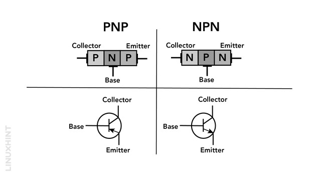
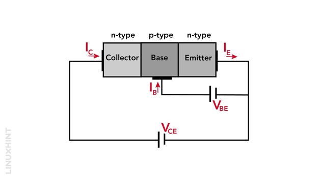
BJTs are further divided into NPN & PNP types. The operation is almost the same, with a difference in polarity and biasing arrangements. NPN Transistor biasing arrangement and circuit diagram are shown below:
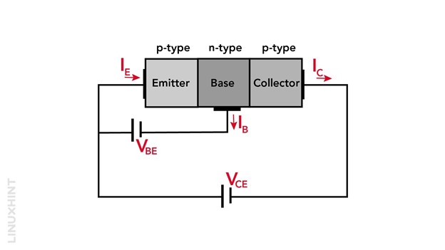
PNP Transistor biasing arrangement and circuit diagram are shown below:
Operating Modes
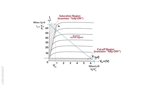
There are three basic modes of transistor operation: cutoff, saturation & active modes shown in the below figure. They are briefly explained below:
Active Mode
The collector emitter-base junction is reverse-biased in the active state compared to the emitter-base junction. From the emitter to the collector, the current flows, and the following conditions apply in the active mode:
Saturation Mode
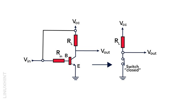
The emitter-base junction and collector-base junction are both forward-biased in saturation mode. The transistor acts as a closed switch and is considered to be in the on-state as shown in the figure below.:
The following conditions apply in saturation mode:
Vin is connected to VCC.:
In the saturation region:
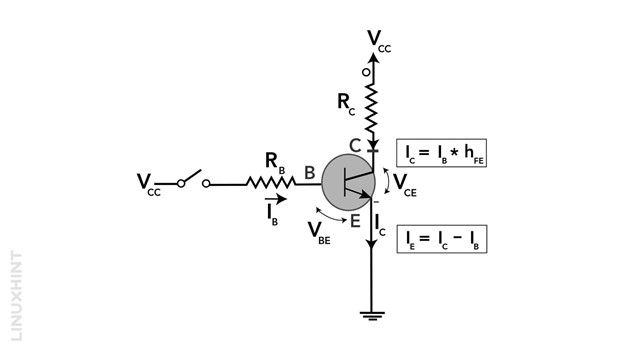
The collector current is expressed as
Cut-Off Mode
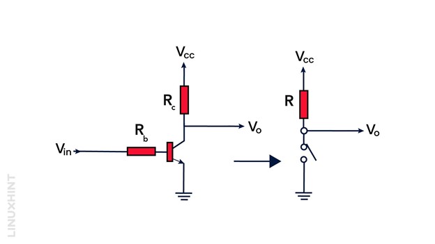
In cut-off mode, the biasing arrangement is opposite to the ones in the saturation mode. The connections at the emitter-base and collector base are both reverse-biased in this mode. The transistor is believed to be operating as an open switch and is expected to be in the off state, as seen below:
The following conditions apply in cut-off mode:
Vin is not connected to VCC.:
In the cut-off region:
Collector current:
NPN Transistor Operation as a Switch
When a voltage is added to the base of an NPN transistor, it functions as a close switch; when the voltage is removed, it opens. The voltage applied at the base shall not be less than 0.7V for forward biasing the base terminal. As shown below, the base of the device is wired for supply voltage, the emitter is grounded, and the collector is wired for external resistance.
PNP Transistor Operation as a Switch
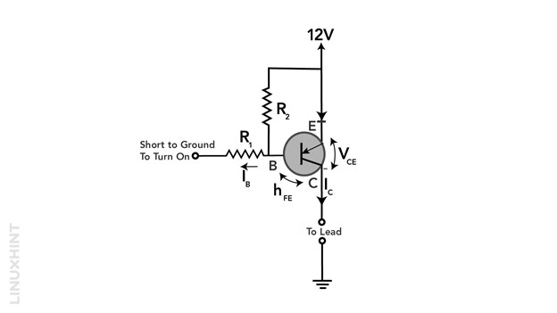
PNP transistors operate as a switch when the base terminal is reverse-biased at 0.7V. The load here is connected between the transistor and ground potential. The voltage applied at the base terminal shall not be less than 0.7V for reverse biasing the base terminal.
For PNP Transistors, the supply voltage is connected to the emitter, while the collector is grounded with an external resistance as shown below:
Note:
The majority of the variations between NPN and PNP transistors can be attributed to the following factors:
- NPN Transistors are forward-biased, while PNP Transistors are reverse-biased for switching operations.
- Charge carriers are electrons in NPN and holes in PNP transistors.
- Current will flow in the path of the collector towards the emitter in NPN and from the emitter towards the collector in PNP.
Conclusion
NPN Transistors act as a closed switch in the saturation region when the voltage is applied at base terminals, and act as an open switch when the voltage is removed. PNP transistors act in the same way, but the negative potential is applied at its base as compared to NPN transistors.

