Sequential Logic Circuit
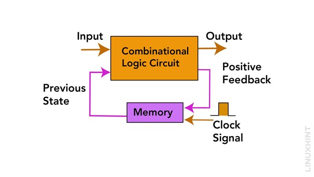
Sequential Logic circuits are the combinational logic circuits with memory units. These circuits are not fully dependent on the input states to provide the output. They are bi-state logic circuits, which means these circuits can maintain the output constantly at high ‘1’ or low ‘0’ even if the inputs are changing with time. The output state can only be changed through an application of trigger pulse in sequential circuits.
The basic representation of sequential circuit is shown below:
Classifications of Sequential Circuits
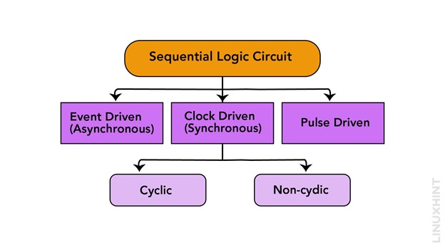
Sequential circuits are divided on the basis of their triggering states, as mentioned below:
- Event Driven Sequential Circuits
They belong to a family of asynchronous sequential logic circuits. They are clockless and can operate immediately on receiving input. The output changes immediately with input combination. - Clock Driven Sequential Circuits
They belong to a family of synchronous sequential logic circuits. These sequential circuits are clock driven. It means that they require a clock signal to operate with input combinations and produce output. - Pulse Driven Sequential Circuit
These sequential circuits can be clock-drive or clockless. In fact, they combine properties of both event & clock driven sequential circuits.
The term ‘synchronous’ means that a clock signal can alter the states of the sequential circuit without applying any external signal. While in asynchronous circuits, an external input signal is needed to reset the circuit.
The term ‘cyclic’ means that a portion of output is being fed back to the input as a feedback path. However, ‘non-cyclic’ is opposite of the cyclic, representing there are no feedback paths in the sequential circuits.
Examples of Sequential Circuits – Latches & Flip Flops
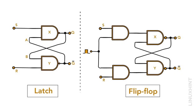
Both latches and flip-flops are sequential circuits, with certain differences in their operation principles. A latch does not include clock signals for triggering states, while the flip-flops require clock triggering as shown in below figure:
The above figure represents SR latch and SR flip-flop. A clock pulse is shown in the case of flip-flop above.
SR Flip Flop
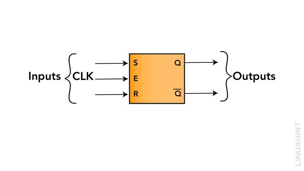
An SR flip-flop is just like an SR latch, with an additional clock function. The clock trigger functions to set the flip-flop in on condition, and the flip-flop behaves dead in the absence of clock pulse.
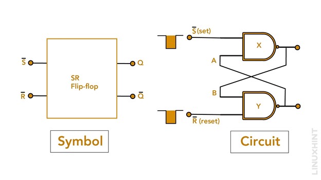
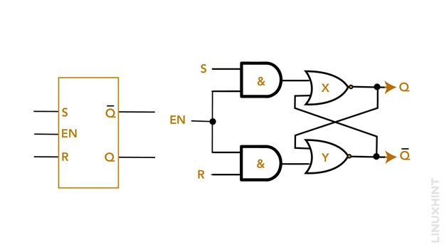
The block diagram of SR Flip Flop is shown below:
Circuit Diagram
SR flip-flops are basically composed of NAND gates, just like SR latch. However, a clock input is indicated between the first two NAND gates to indicated clock triggering as indicated below:
Truth Table
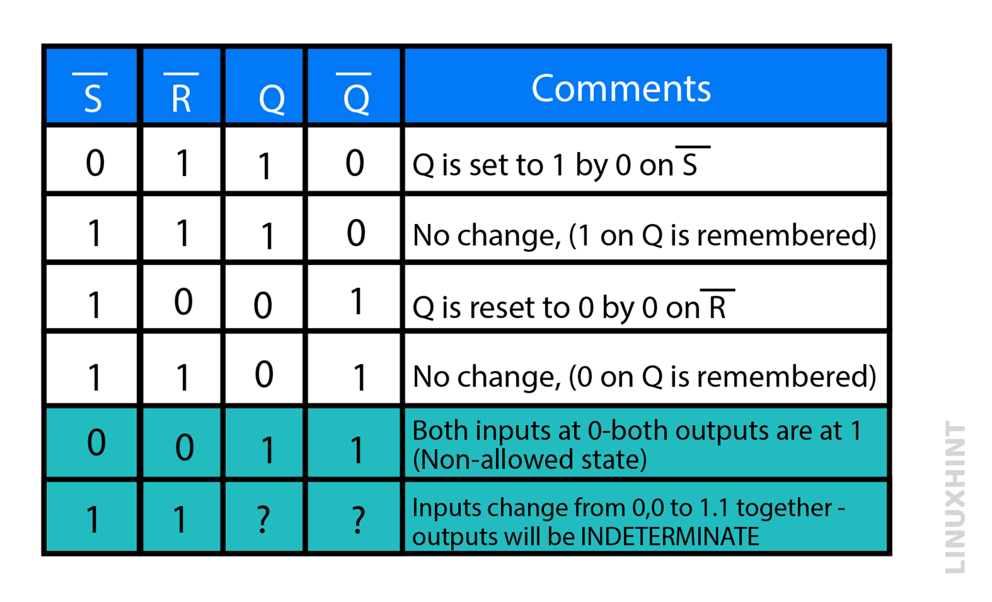
The truth table comprising all the four possible input combinations at S & R terminals along with two outputs states, Q & Q is tabulated below:
The clock input is kept always at E=1 to enable the operation of the SR flip-flop. The four combinations of inputs and outputs are discussed below:
1: When S=0, R=1 (Set):
The output Q achieves high state when S=0 & R=1
2: When S=1, R=0 (Reset):
The output Q turns zero while output Q’=1 when S=1 & R=0.
3: When S=1, R=1 (No Change):
The output remains in its previous state as recalled by the SR flip flop.
4: When S=0, R=0 (Indeterminate):
The outputs are indeterminate as both inputs are low.
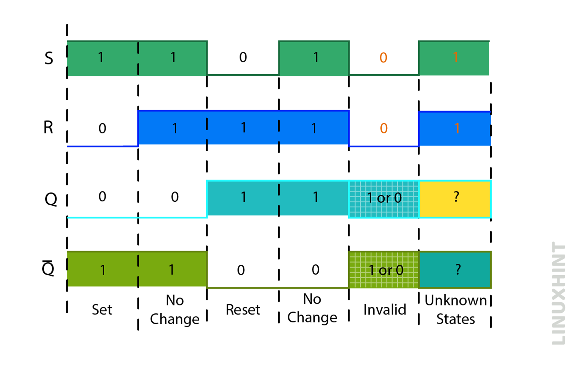
Switching Diagram
The SR flip-flop switching diagram can be plotted below for high and low states of ‘S’ & ‘R’ inputs with outputs. The switching diagram seems fine until both input states turn to ‘0’ and the outputs become invalid. After the invalid state, the SR flip-flop becomes unstable while one output may switch faster than the other, resulting in indeterminate behavior.
Types of SR Flip Flop:
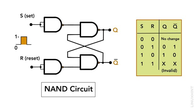
SR flip flops can be built using AND, NAND, and NOR gate. The configuration details along with truth tables of each type are discussed below.
1- Positive NAND Gate SR Flip Flop
Positive NAND gate flip-flop adds two extra NAND gates in the basic SR flip-flop. The positive NAND gate switches to set and reset states by applying a high input instead of low inputs in basic SR flip-flop. In other words, an input of ‘1’ at ‘S’ terminal shall provide a set state, while an input of ‘1’ at ‘R’ terminal shall provide a reset state.
Moreover, the case of invalid state now appears when both inputs are high while both zero inputs have no change in outputs.
2-NOR Gate SR Flip Flop
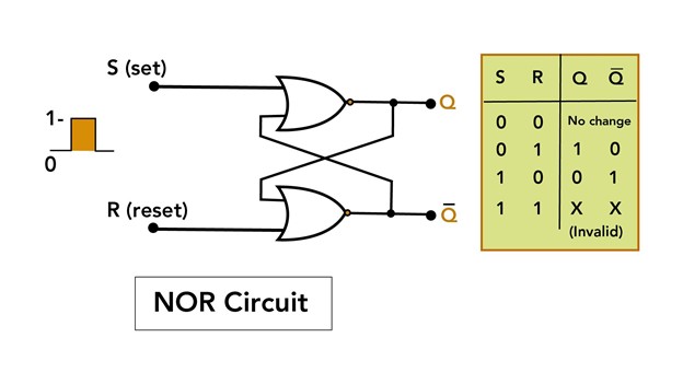
SR flip-flops can also be constructed using two NOR gates. This configuration works similar to positive NAND gates configuration. The set and reset states are triggered by high pulse or ‘1′ instead of low pulse or ‘0’ in basic SR flip-flop configuration. The truth table shows the same output states as of positive NAND gate SR flip-flop.
3-Clocked SR Flip Flop
Clocked SR flip flops take their inputs from two AND gates. One of the inputs of the AND gate is the input signal for terminals of SR flip flop while the second input is clock or enable. Clock pulse plays a significant role in this configuration. The clock pulse can switch two extra NAND gates to turn on or off as required to provide better control on output state. When enable input ‘EN’ is high, all of the NAND gate functions provide output. When enable input ‘EN’ is low, the two extra NAND gates are disconnected, and previous states are recalled by the SR flip flop.
Application – Switch Debounce Circuit
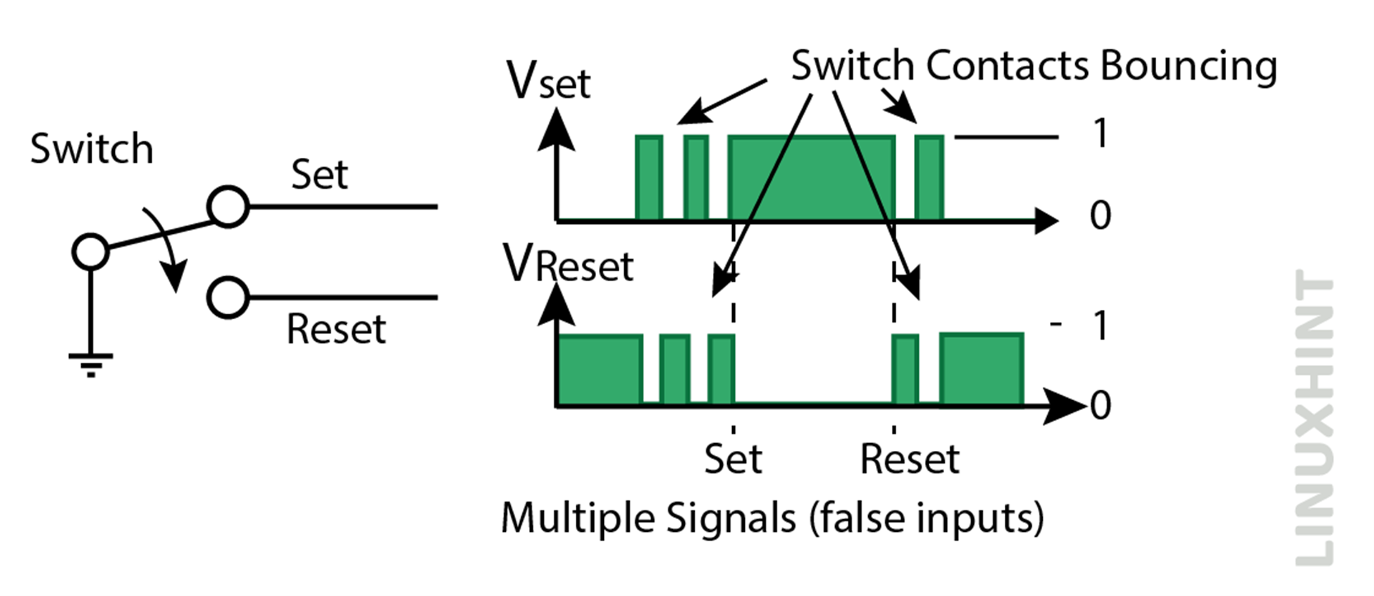
SR flip flops are edge triggered and they switch their states quite smoothly. They can eliminate the bouncing of mechanical switches. The phenomenon of bouncing occurs when the external mechanical switch does not operate internal contacts completely and the contacts bounce before they are closed or opened. This process creates an array of unwanted signals which can trigger logic gates unexpectedly before the actual inputs are applied.
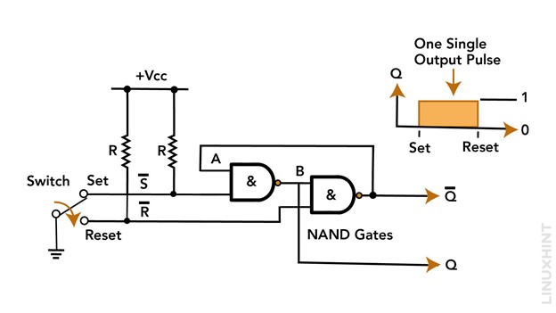
In the switch debounce configuration, contacts of the mechanical switch are connected with set and reset terminals of a basic SR flip flop as shown below:
As SR flip flops are edge triggered, the starting input state will count towards the generation of output, regardless of fluctuations in the input later. Even if an array of close-open states occurs due to switch bouncing as shown below, the output shall still be one smooth pulse.
Conclusion
Sequential logic circuits differ from combinational circuits on the basis of memory units. These logic circuits depend on the past input states as well along with present input states. These circuits can maintain their output states at high or low levels even if the inputs change with time. The most common example of sequential logic circuits are SR flip flops. They are just like SR latch with additional memory units.

