MOSFET Amplifier
A MOSFET amplifier is based on Metal-Oxide-Semiconductor technology. It is a kind of insulated-gate based field-effect transistor. Field-effect transistors provide lower o/p impedance and a higher i/p impedance when utilized for amplification functions.
Circuit & Operation of Enhancement MOSFET Amplifier
The circuit for a MOSFET amplifier is given below. The letters ‘G,’ ‘S,’ and ‘D’ are used in this circuit to indicate the positions of the gate, source, and drain while the drain voltage, the drain current and gate-source voltage have been represented by VD, ID, and VGS.
MOSFETs often operate in three regions, linear/ohmic, cut-off and saturation. When MOSFETs are used as amplifiers, they function in the ohmic zone of one of these three operating regions, where the device’s overall current flow increases as the applied voltage rises.
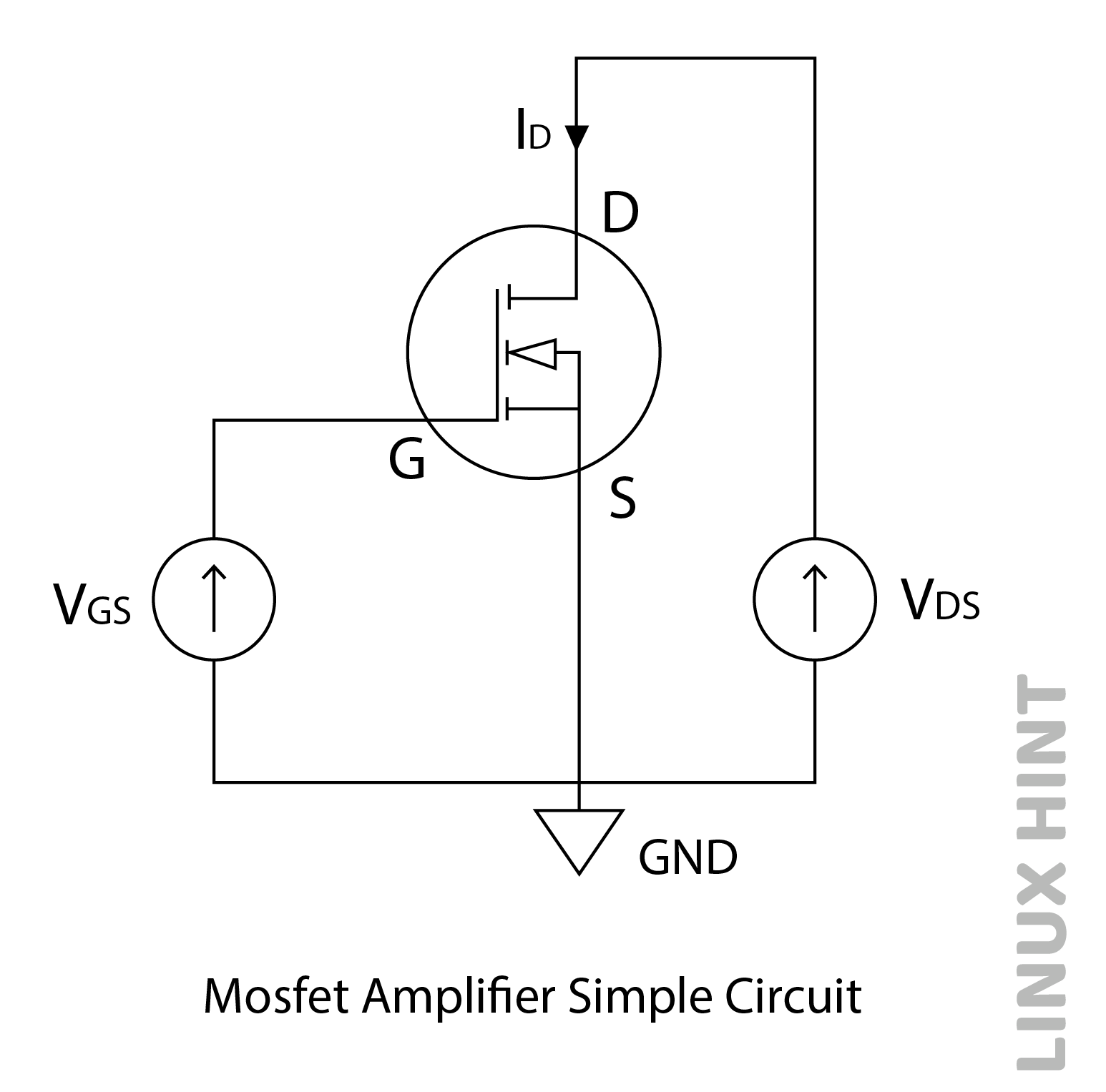
In the MOSFET amplifier, similar to a JFET, a little change in gate voltage will result in a significant change in its drain current. As a result, MOSFET serves as an amplifier by strengthening a weak signal at gate terminals.
Working of MOSFET Amplifier
MOSFET amplifier circuit is created by adding a source, drain, load resistor, and coupling capacitors to the simpler circuit shown above. The MOSFET amplifier’s biasing circuit is provided below:
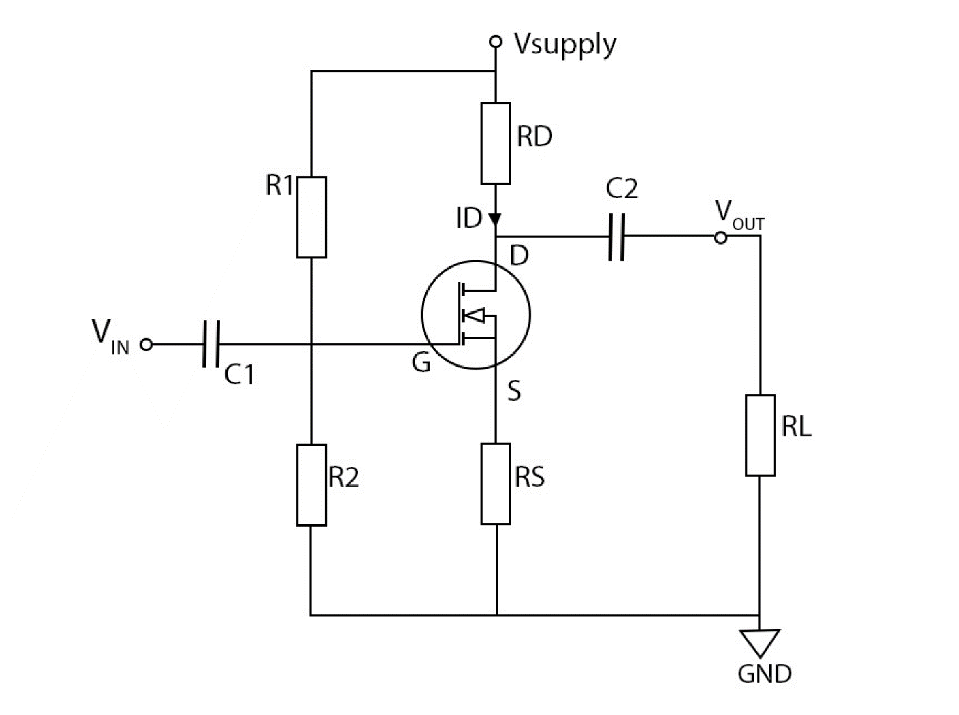
A voltage divider is the building component of the above biasing circuit, and its primary job is to bias a transistor in one direction. Therefore, this is the biasing technique that transistors use in the most commonly biased circuits. To ensure that voltage is divided and delivered into the MOSFET at the proper levels, two resistors are used. Two parallel resistors, R1 and R2, are used to deliver the bias voltages. The biasing DC voltage divider in the above circuit is shielded from the AC signal that will be amplified further by the C1 and C2 pair of coupling capacitors. The load as an RL resistor receives the output. The biased voltage is given by:

R1 and R2 values are typically high in this case to increase the amplifier’s input impedance and to limit ohmic power losses.
Input and Output Voltages (Vin & Vout)
We assume that there is no load connected in parallel to the drain branch in order to simplify the mathematical expressions. The source -gate voltage VGS, receives the input voltage (Vin) from the gate (G) terminal. RS x ID shall provide the voltage drop across the respective RS resistor. Transconductance (gm) is the ratio of drain current ( ID) to gate-source voltage ( VGS) after a constant drain-source voltage has been applied:

So, ID = gm×VGS & the input voltage (Vin) may be calculated from VGS :

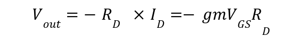
The o/p voltage (Vout) in the above circuit is:
Voltage Gain
The voltage gain (AV) is the ratio of input and output voltages. Following that reduction, the equation will become:

The fact that the MOSFET amplifier performs inversion of the o/p signal just like the BJT CE Amplifier. The symbol “-“ accounts for inversion. The phase shift is thus 180° or rad for outputs.
Classification of MOSFET Amplifier
There are three different kinds of MOSFET amplifiers: common gate (CG), common source (CS), and common drain (CD). Each type and its configuration are detailed below.
Amplification Using Common Source MOSFETs
In a common source amplifier, the o/p voltage is amplified, and it reaches across the resistor at the load inside the drain (D) terminal. The i/p signal is provided at both the gate (G) and source (S) terminals in this case. The source terminal serves as a reference terminal between the i/p and o/p in this arrangement. Due to its high gain and potential for more signal amplification, this is particularly preferable configuration that BJTs. Below is a diagram of a common source MOSFET amplifier’s circuit.
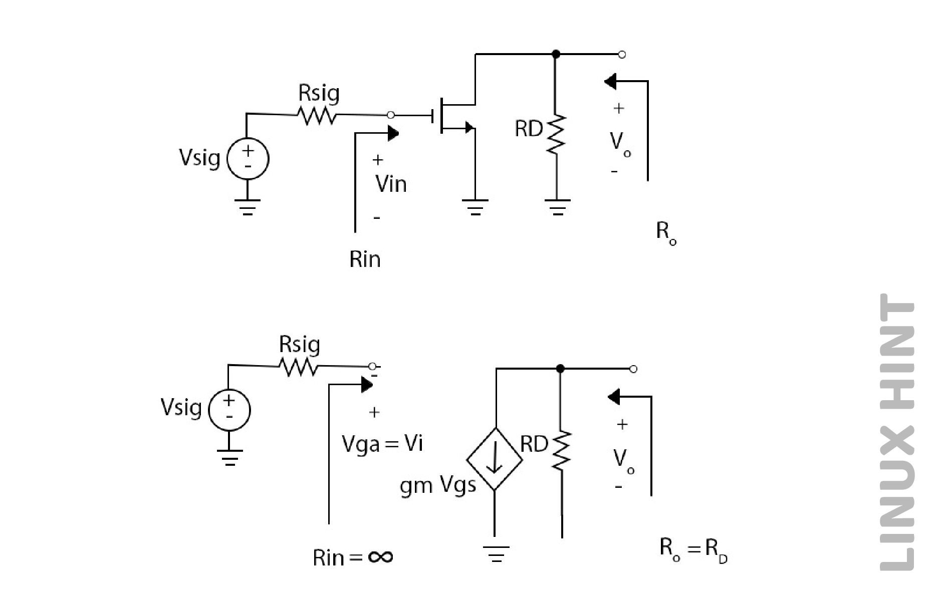
The “RD” resistor is the resistance between the drain (D) and ground (G). The hybrid π model, which is shown in the next figure, is used to represent this small-signal circuit. From this model, current produced is represented by i = gmvgs. Therefore,

The values of different parameters can be estimated to be Rin=∞, Vi=Vsig and Vgs=Vi
Thus, the open-circuit voltage gain is:

A linear circuit powered by a source may be swapped out for its Thevenin or Norton’s equivalent. Norton’s equivalency can be used to modify the circuit’s output portion from the small-signal circuit. The Norton equivalent is more practical in this situation. With the assumed equivalency, the voltage gain GV can be modified as:

Common Source MOSFET amplifiers have infinite input/output impedance, high on/off resistance, and high voltage gain.
Common-Gate Amplifier (CG)
Common-gate (CG) amplifiers are often used as current or voltage amplifiers. The transistor’s source terminal (S) functions as the input in the CG arrangement, while the drain terminal serves as the output and the gate terminal is linked to ground (G). The same gate amplifier arrangement is often used to create strong isolation between the input and output to reduce input impedance or avoid oscillation. The common-gate amplifier equivalent circuit’s small-signal and T models are shown below. The gate current in the ‘T’ model is always zero.
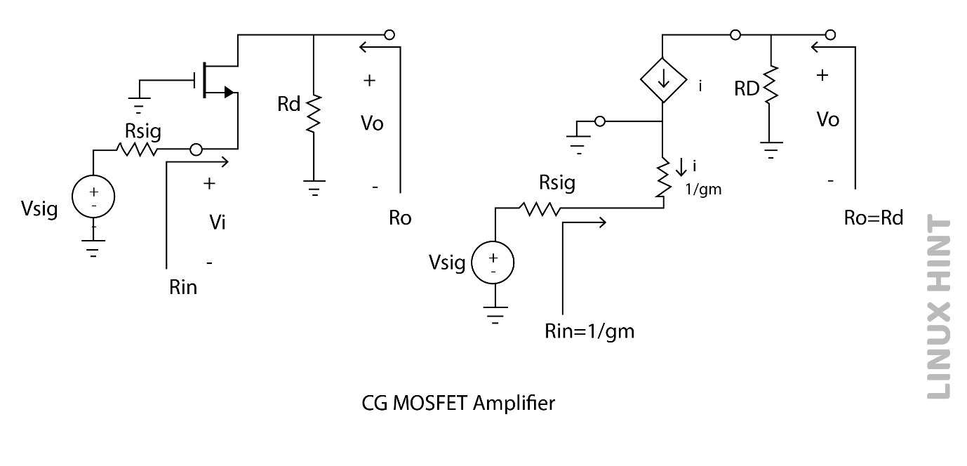
If, ‘Vgs’ is applied voltage and the current at the source is represented by ‘Vgsx gm’, then:

Here, the common gate amplifier has reduced input resistance represented as Rin = 1/gm. The value of input resistance is generally a few hundred ohms. The o/p voltage is given as:

Where:

Therefore, the open-circuit voltage may be represented as:

As the output resistance of the circuit is Ro = RD, the amplifier gain suffers from the low i/p impedance. Therefore, using the voltage divider’s formula:
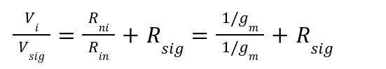
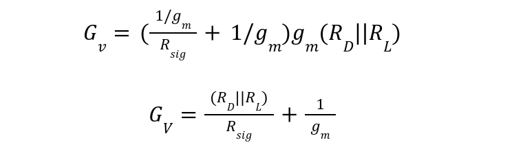
Because ‘Rsig’ is often greater than 1/gm, the ‘Vi’ is attenuated in comparison to Vsig. The appropriate voltage gain is achieved when a load resistor ‘RL’ is connected to the o/p,. The voltage gain is thus represented as:
Common Drain Amplifier
A common-drain (CD) amplifier is one in which the source terminal receives the output signal, and the gate terminal receives the input signal while the drain (D) terminal is left open. Small o/p loads are frequently driven using this CD amplifier as a voltage buffer circuit. This configuration offers very low o/p impedance and extremely high i/p impedance.
The common drain amplifier’s equivalent circuit for small signals and the T model is displayed below. The i/p input source in this circuit can be identified by the equivalent voltage of a resistor (Rsig) and a Thevenin (Vsig). A load resistor (RL) connects with output in between the source (S) terminal & ground (G) terminal.
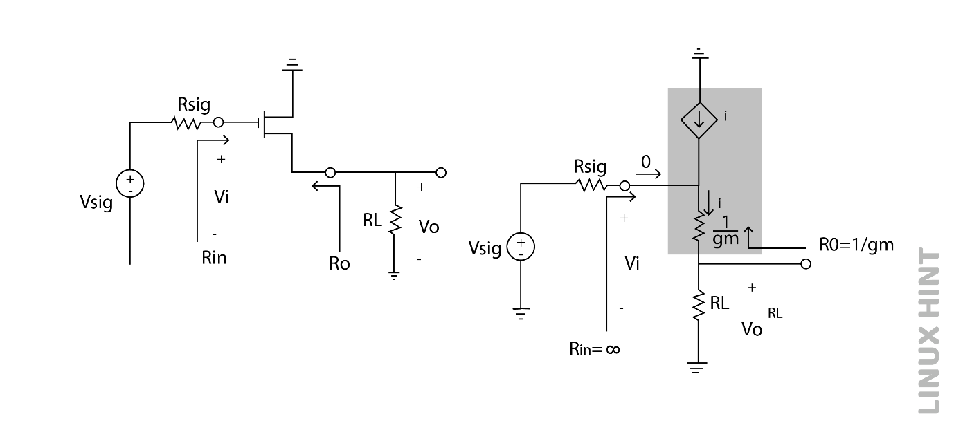
Since the IG is zero, Rin = ∞ The voltage divider for terminal voltage can be expressed as:

By using Thevenin’s equivalent, overall voltage gain is found similar to above expression, which can be evaluated while considering R0=1/gm as:

Since Ro = 1/gm is generally quite a small value from large load resistor ‘RL’, the gain is smaller than unity in this case.
Conclusion
The difference between a regular amp and a MOSFET amp is that a regular amp uses an electronic circuit to amplify the input signal to produce an output signal with a high amplitude. MOSFET amplifiers process digital signals with comparatively little power consumption as compared to BJTs.