Light-emitting diodes are the most common light-producing elements in every electronic appliance just for indication. LEDs are composed of P-type and N-type materials with a heavy proportion of impurities doping in them. LEDs are usually enclosed in a transparent cover, and they can produce a wide range of colored lights at different wavelengths.
What is a Light Emitting Diode (LED)
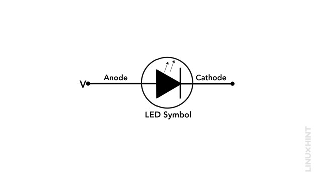
An LED is composed of a single PN junction which produces light when it is connected in a forward-biased arrangement. The PN junction of LED differs from normal PN junctions on the grounds of the selection of semiconductor alloys and the proportions of doping in them. The gallium-based alloys together with heavy amounts of doping. The symbol of LED is shown below:
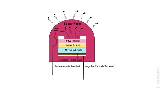
Construction of Light Emitting Diode (LED)
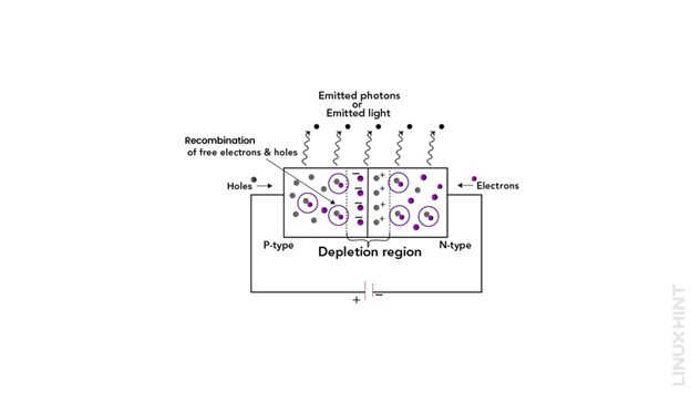
An LED comprises particular gallium semiconductor compounds (GaAs, GaP) that produce light upon recombination of major charge carriers with minority charge carriers as soon as the forward bias arrangement is applied. The simple circuit of the LED PN junction with the forward biasing arrangement is shown below:
The heavy doping of P-type and N-type material gives rise to increased amounts of holes and electrons in both of the semiconductor materials. The excess charge carriers lead to an increased rate of minority charge accumulation at the depletion layer.
Working of Light Emitting Diode (LED)
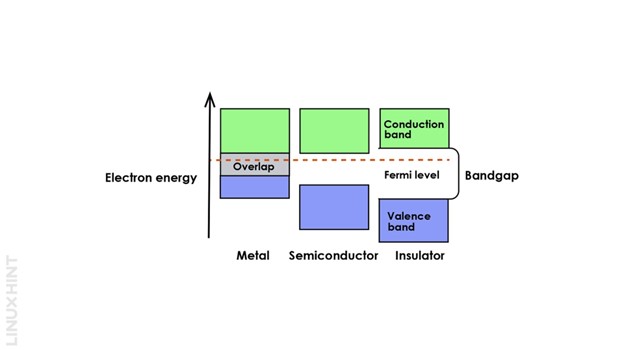
In any semiconductor material, the electrons can exist in three types of energy levels. The valence shell electrons of all the atoms exist in the valence energy band. However, as soon as an external supply is applied, these electrons move to the conduction band.
The inter-band gap changes for different materials. Consequently, the gap between bands will vary for semiconductors, insulators, and conductors. It is highest in insulators, so there are rare chances that electrons will jump from valence to conduction bands.
Another energy level known as the Fermi level exists between valence and conduction energy bands. Electrons at this level are present when the temperature falls to zero kelvin. Fermi levels are considered as lower energy states slightly above the valence band levels.
When the positive potential is applied at the P-type end, the minority charge carriers, which are free electrons, are pushed toward the junction end. Similarly, when a negative potential is connected at the N-type end, the minority charge carriers present in the material, which are holes, are pushed toward the junction end. This forms a barrier of charges at the junction point, shown below:
This barrier of charges at the junction is called the depletion layer. As soon as the forward bias voltage of 0.7V is applied, two changes occur in the PN junction. First, electrons achieve higher energy to move freely in the conduction band, releasing energy in the form of light. Second, the barrier is removed. After the barrier vanishes, the minority carriers within the barrier start to recombine with the majority carriers, resulting in the conduction of current across LEDs.
Color Scheme of Light Emitting Diode (LED)
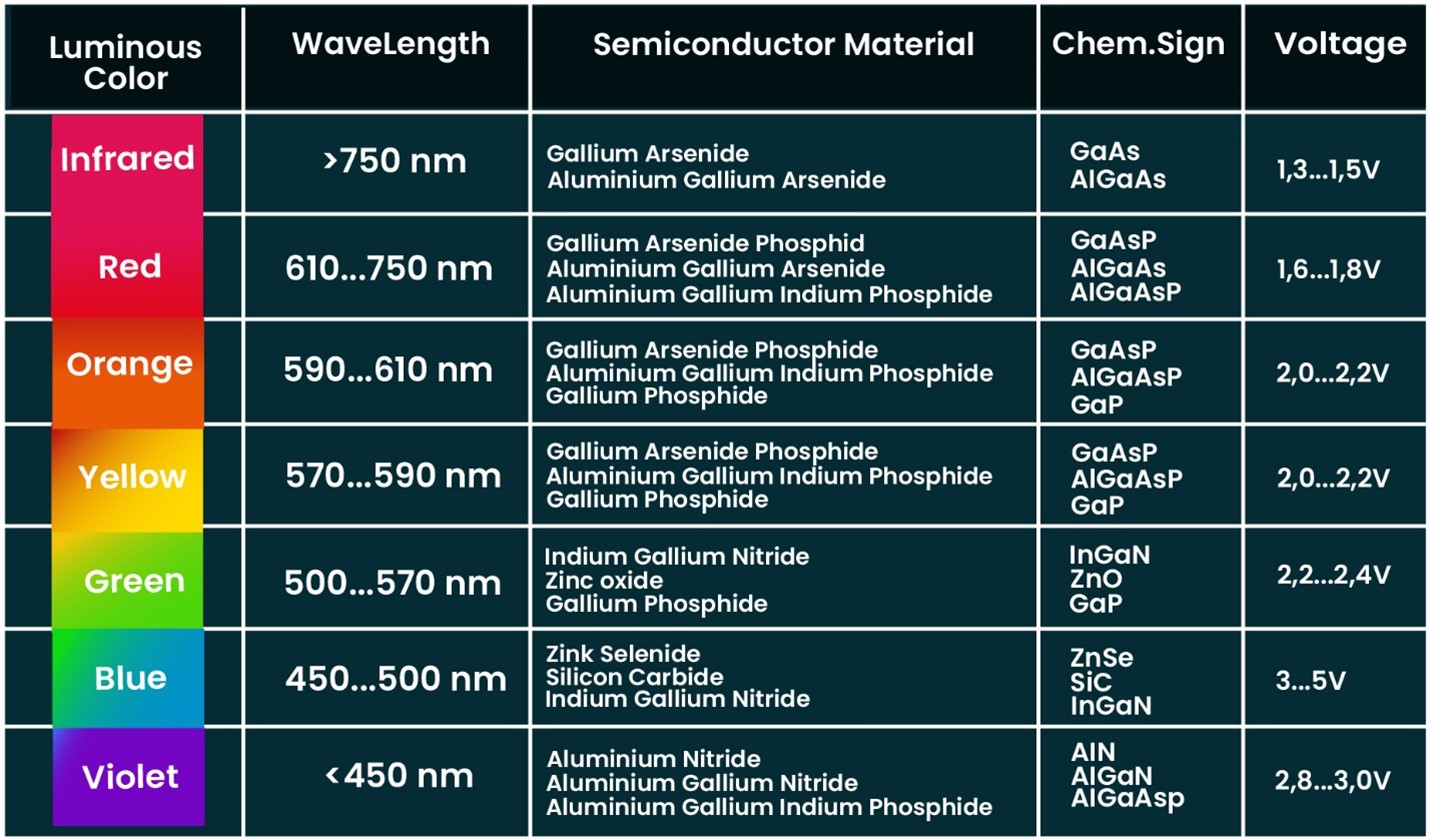
The type of color produced by LED is based on the semiconductor material used in its construction. The typical alloys used in LEDs range from aluminum, indium, phosphides, and gallium. The color scheme for these compounds is as below:
Conclusion
LEDs are PN junctions composed of semiconductor alloy materials that produce light when forward biasing is applied across its terminals. LEDs can produce different color schemes depending on the types of alloys used in their construction.

