The Insulated Gate Bipolar Transistor
The Insulated Gate Bipolar Transistor (IGBT) uses high switching speeds of MOSFET and less saturation voltage of BJT and combines both of them to make a transistor that has a high switching speed and can handle large amounts of current.
The term ‘insulated gate’ also indicates the high input impedance characteristic of MOSFET is also
incorporated in IGBT. Similarly, it is also a voltage-controlled device like MOSFET. The term ‘bipolar transistor’ indicates the output characteristics of BJT are included in IGBT.
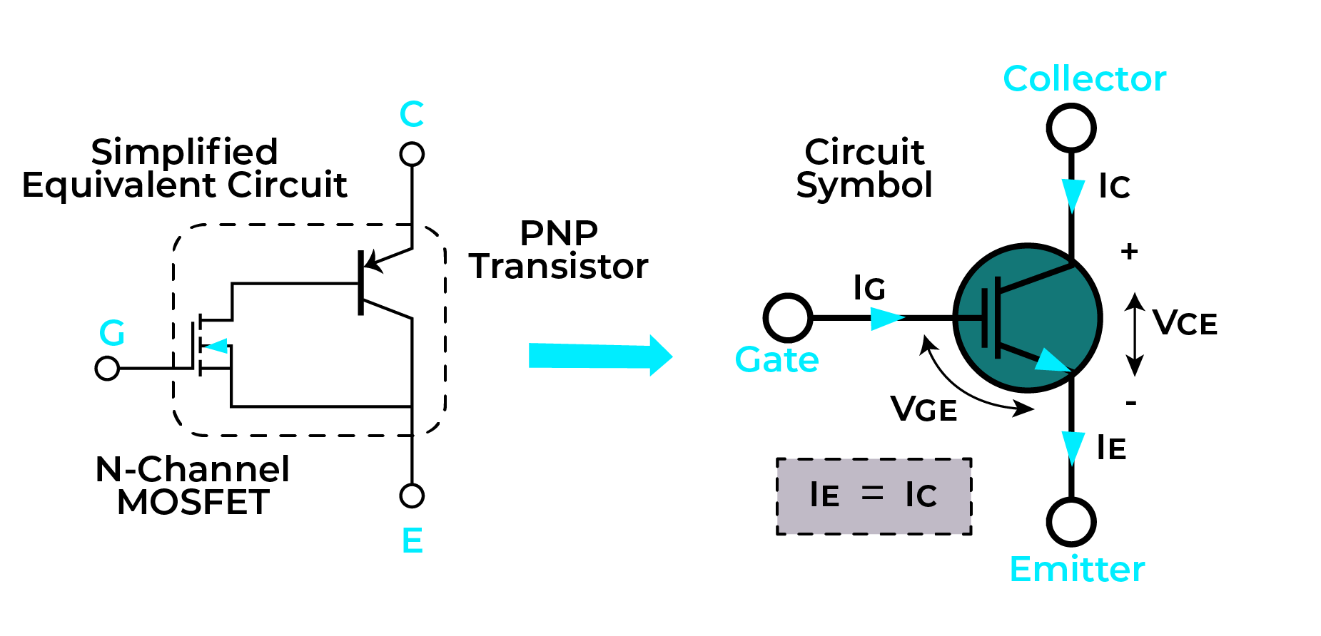
These characteristics are responsible for the greater power gain than both BJT and MOSFET. The configuration of IGBT can be shown as a combination of MOSFET and BJT with the source of MOSFET connected to the base of BJT as shown below. The circuit symbol of IGBT is also given below.
Construction of IGBT
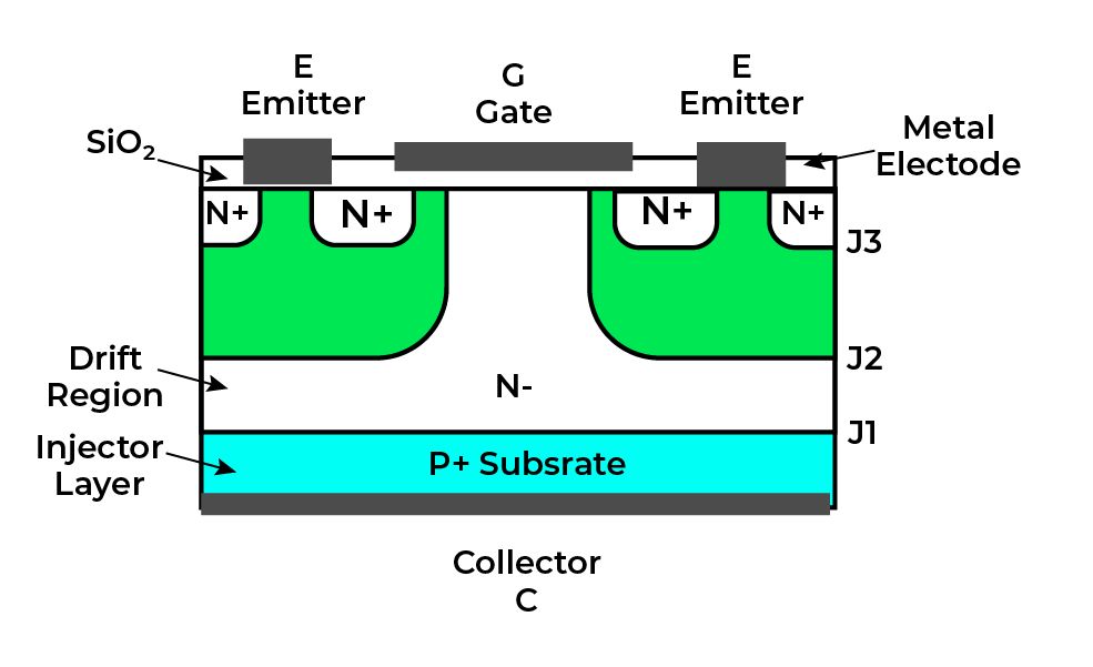
Insulated Gate Bipolar Transistor consists of four different layers of semiconductors arranged in the form of PNPN layers. The collector of IGBT is attached to the P+ layer also known as the injection layer. This P+ is a substrate, which means that it is lightly doped. On top of the P+ layer is an N- layer, which is also called the drift region because electrons slowly move in this area. These P+ and N- layers form junction J1 as shown in the figure.
There are two P-layers on top of the N- layer. They are placed in such a design that a path is left between them for the gate electrode. The gate electrode is linked to the N- layer via the insulation of Silicon Dioxide SiO2. These layers form junction J2 with the N- layer. On top of two P-layers, there are N+ layers that are connected to the emitter.
The P+ layer is used for injecting holes in the N- layer. The N- layer then provides a path for current flow between the collector and emitter.
Working of IGBT
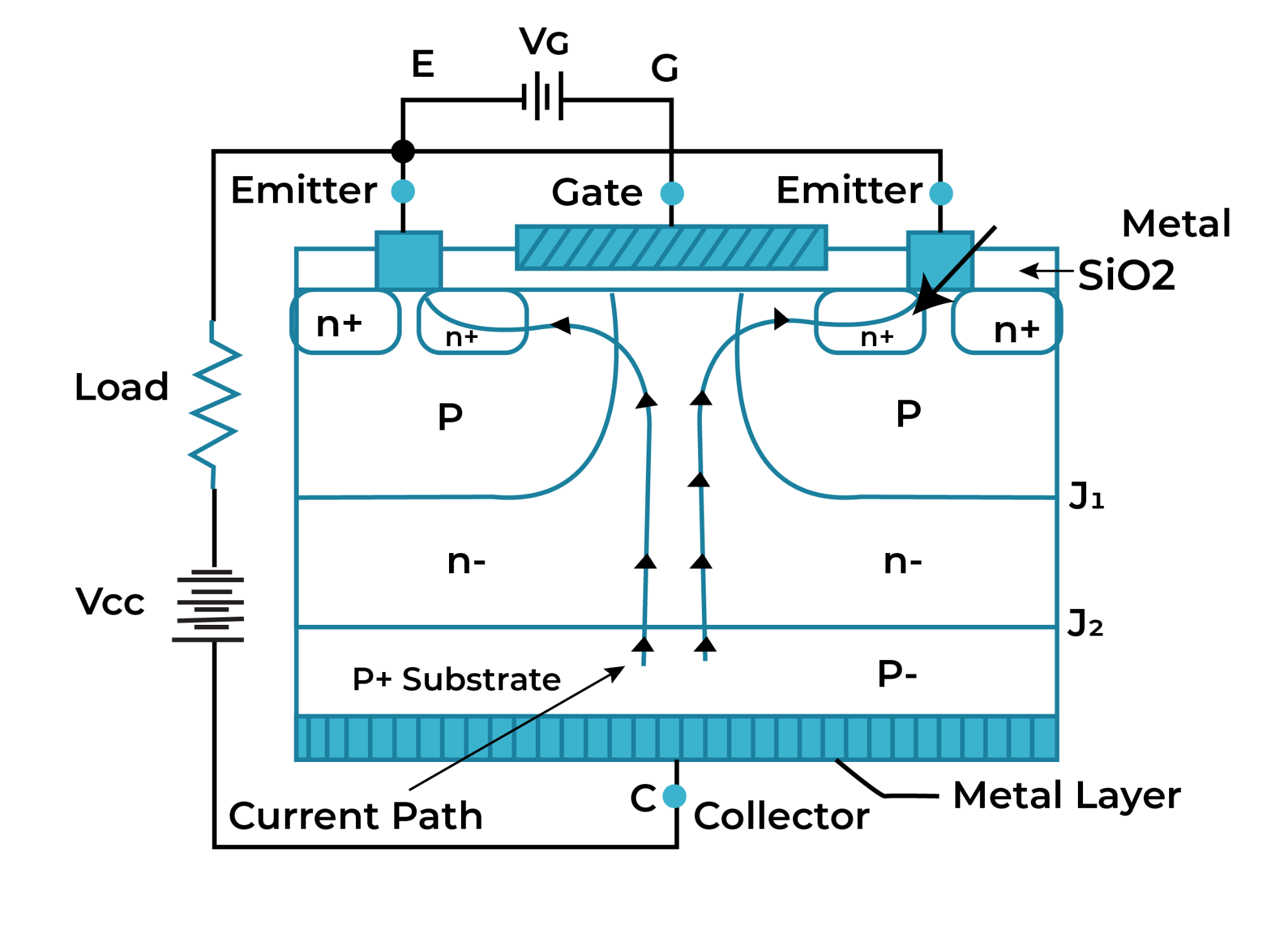
IGBT conducts current from collector to emitter, whereas the gate is used for voltage control of IGBT. The working of IGBT depends on the biasing of its junctions. As the figure below shows, the collector is connected to the positive terminal of VCC, and the emitter is connected to the negative terminal of VCC through the load resistance. This makes the emitter more negative than the collector, and junction J2 gets reverse biased and junction J1 gets forward biased. Here, in such a condition, IGBT is turned OFF as there is no signal on the gate terminal.
When VG is applied to the gate terminal, a capacitance is built in the SiO2 layer due to the positive charge at the gate and a negative charge at the N+ layers. When Gate-Emitter voltage VG is further increased and crosses the threshold voltage, electrons from the N+ layer start flowing towards the N- layer and simultaneously P+ layer starts injecting holes in the N- layer. When there are plenty of holes and electrons in the drift region, IGBT turns ON and starts conducting.
Current-Voltage (I-V) Characteristics of IGBT
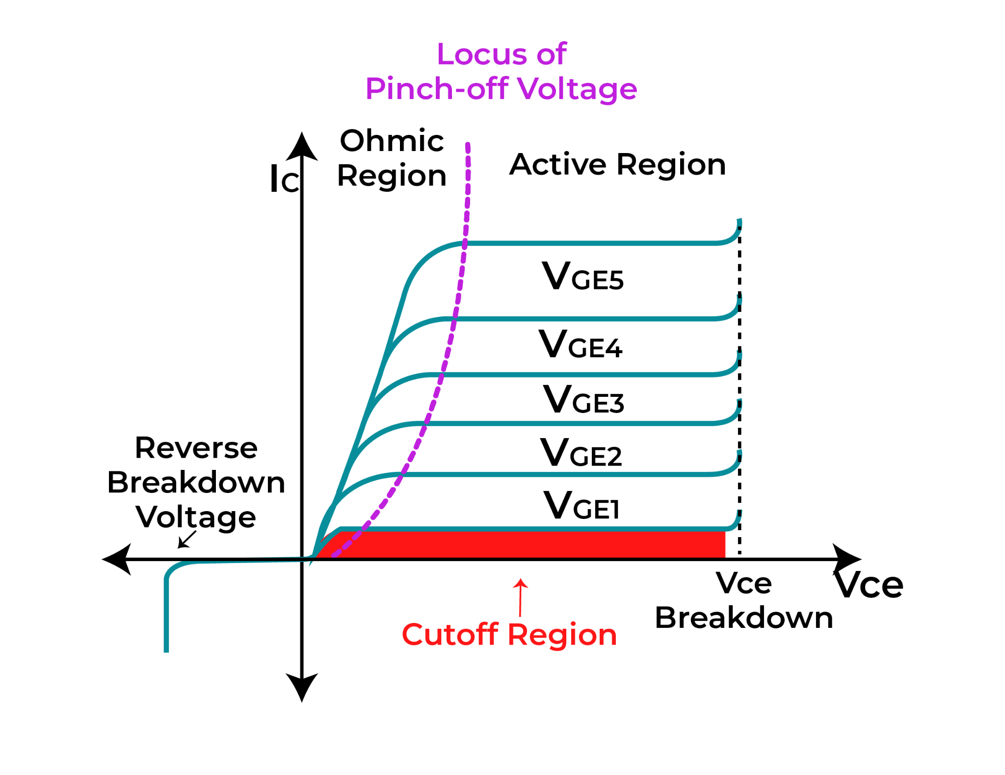
The current and voltage characteristics of IGBT have three main stages: cut-off, active region, and saturation region. The other two stages are avalanche breakdown and reverse breakdown.
Cut-Off Region
Initially, when no voltage is applied at the gate, no collector current flows in IGBT and the transistor is switched OFF. When the voltage at the gate terminal is applied but is lower than the threshold voltage, IGBT remains OFF, but there is a small leakage current in the forward direction. The device is said to be in the cut-off region in both of the above-mentioned conditions.
Active Region
When Gate-Emitter Voltage VGE is increased beyond the threshold voltage, the device goes into the active region and starts conducting. In the active region, IGBT has a low input voltage drop and the output current starts increasing.
Saturation Region
As we know that IGBT conducts current in a single direction therefore, after some time, the collector current reaches a maximum level. The collector current keeps rising at different voltage levels of VGE as shown in the figure below. This stage is known as the saturation state or where IGBT is now fully turned ON and is conducting. Therefore, this region is also called an ohmic region.
Avalanche Breakdown
The IGBT encounters avalanche breakdown if the applied voltage VCE exceeds a certain limit. When VCE gets very large, junction J1 can no longer offer resistance or blockage to current and IGBT breaks down to conduct indefinitely.
Reverse Breakdown
In cases where reverse voltage is applied to IGBT, it should not exceed the maximum reverse voltage VRM. When the reverse voltage exceeds VRM, the transistor breaks down and starts conducting, as it can no longer block current in reverse.
Transfer Characteristics of IGBT
In the above diagram, the blue line indicates the transfer characteristics of IGBT. The transfer characteristics express the relation between collector current IC and emitter gate voltage VGE. The locus of pinch-off voltage is the VGE at which maximum collector current can flow through IGBT.
Advantages of IGBT
As IGBT is a combination of MOSFET and BJT, it possesses the benefits of both of them. It has a high input impedance with greater voltage and current carrying capacities. Similarly, it has a high switching speed even with low voltages.
Similarly, IGBT is voltage controlled so, it does not have input current so are the input losses. It has a simple circuit for the signaling gate, and it can be easily switched ON and OFF by applying positive or negative voltages at the gate.
It also possesses high power gain and high current density.
Disadvantages of IGBT
The prominent disadvantage of IGBT is that it is unidirectional and cannot conduct current in the reverse direction. It is also slightly more expensive than MOSFET and BJT, as it is formed by combining both. It cannot block reverse voltage as well. Therefore, IGBT breaks down and conducts indefinitely if reverse voltage becomes high.
Differences Between IGBT and BJT
Some major differences between IGBT and BJT are as follows.
- BJT is a current controlled whereas IGBT is a voltage-controlled device
- The base is the control terminal in BJT and Gate is the control terminal in IGBT
- The switching speed of IGBT is higher than BJT
- The input impedance of BJT is lower than that of IGBT
- BJT has a negative temperature coefficient, whereas IGBT has a positive temperature coefficient
Differences Between IGBT and MOSFET
Some major differences between IGBT and MOSFET are as follows.
- IGBT can handle large voltage and power, whereas MOSFET can handle medium voltage and power
- IGBT is used for low frequencies in kHz and MOSFETs are used for high frequencies in MHz which means the switching speed of MOSFET is higher than IGBT
- The turn-OFF time of IGBT is larger than MOSFET
- IGBT is more costly than MOSFET
- IGBTs are used in high-power AC applications, whereas MOSFETs are used in low-power DC applications
Applications of IGBT
IGBTs are used in solar inverters, converters, variable frequency dividers, speed controllers in motors, and Uninterrupted Power Supply systems. They also supply energy to medical equipment, computers, and laptops.
Conclusion
Insulated Gate Bipolar Transistor is a type of transistor that is a merger of Bipolar Junction Transistor and MOSFET. It utilizes the input characteristics of MOSFET and the output characteristics of BJT. It is constructed by four-layer PNPN structures. It has a high switching speed and high-power gain, but it can only conduct unidirectional. They are extensively utilized in modern-day electronics.


