Building 555 Timer IC-Based Astable Multivibrator
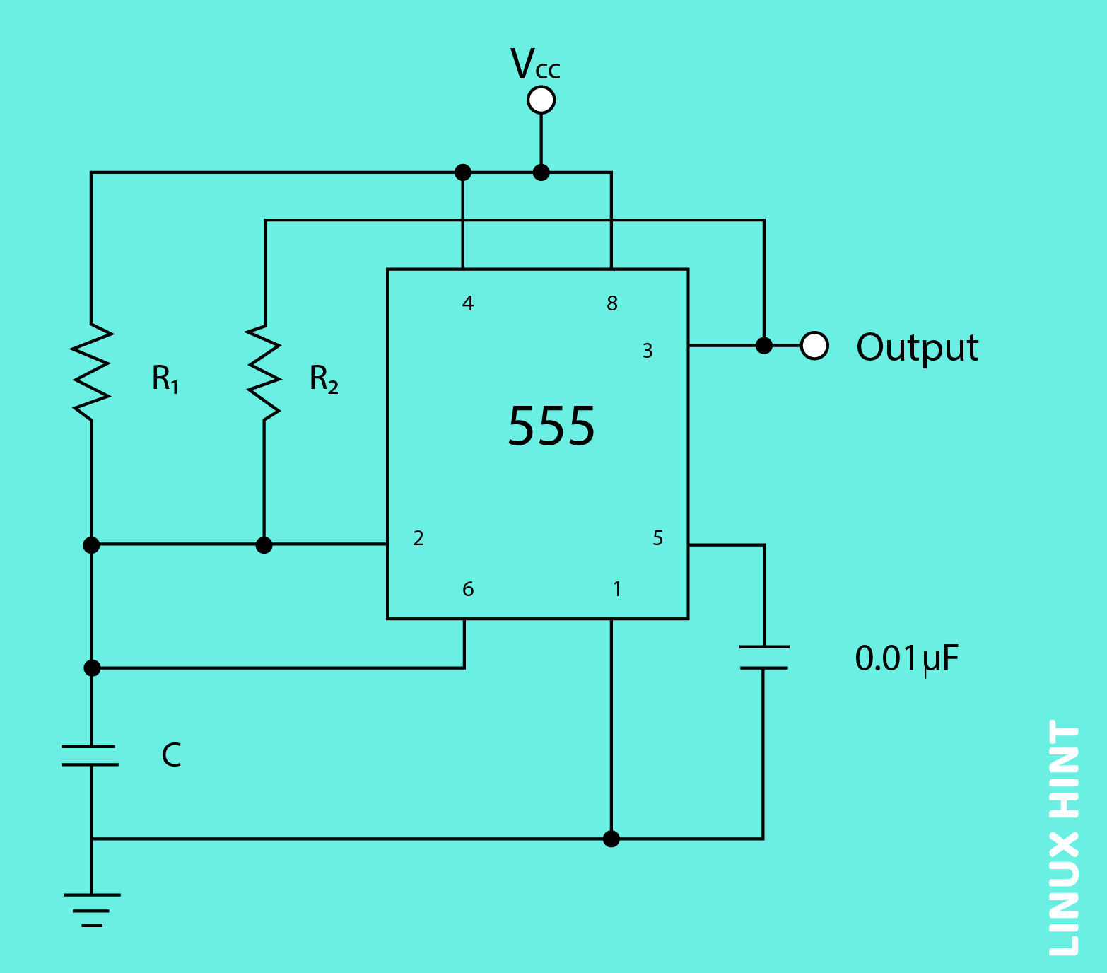
Without the use of any external triggers, 555 timer IC can alternate between its two states. Three additional external parts, two resistors (R1 and R2), and a capacitor (C) may be added to the IC 555 to convert it into an astable multivibrator circuit. The below circuit shows IC 555’s use as an astable multivibrator together with the three external parts.
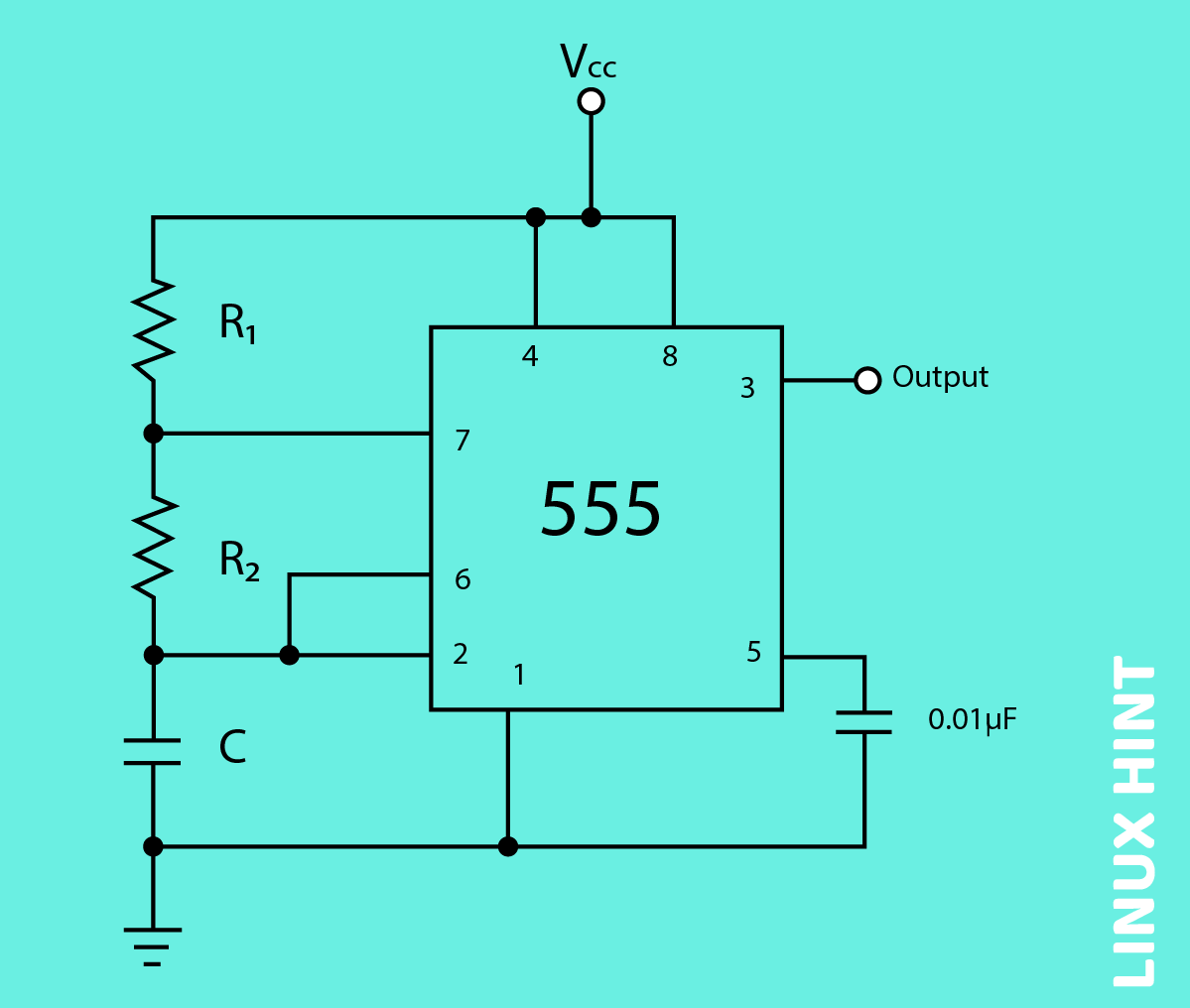
Since pins 6 and 2 are already connected, the device will activate automatically and function as an oscillator without the need for an external trigger pulse. VCC as a supply input voltage is linked to pin 8. Since Pin 3 in the above circuit is the output terminal, the output can be drawn from here. The external reset pin is pin 4 in the circuit, and this pin can restart the timer but usually, pin 4 is connected to VCC when the reset function is not in use.
The threshold voltage level will fluctuate depending on the control voltage provided at pin 5. In contrast, pin 5 is often linked to the ground through a capacitor, which filters out external noise from the terminal. The ground terminal is pin 1. R1, R2, and C make up the timing circuit, which controls the output pulse’s width.
Operation Principle
The IC 555’s internal circuit is displayed in astable mode, with R1, R2, and C all being a part of the RC timing circuit.
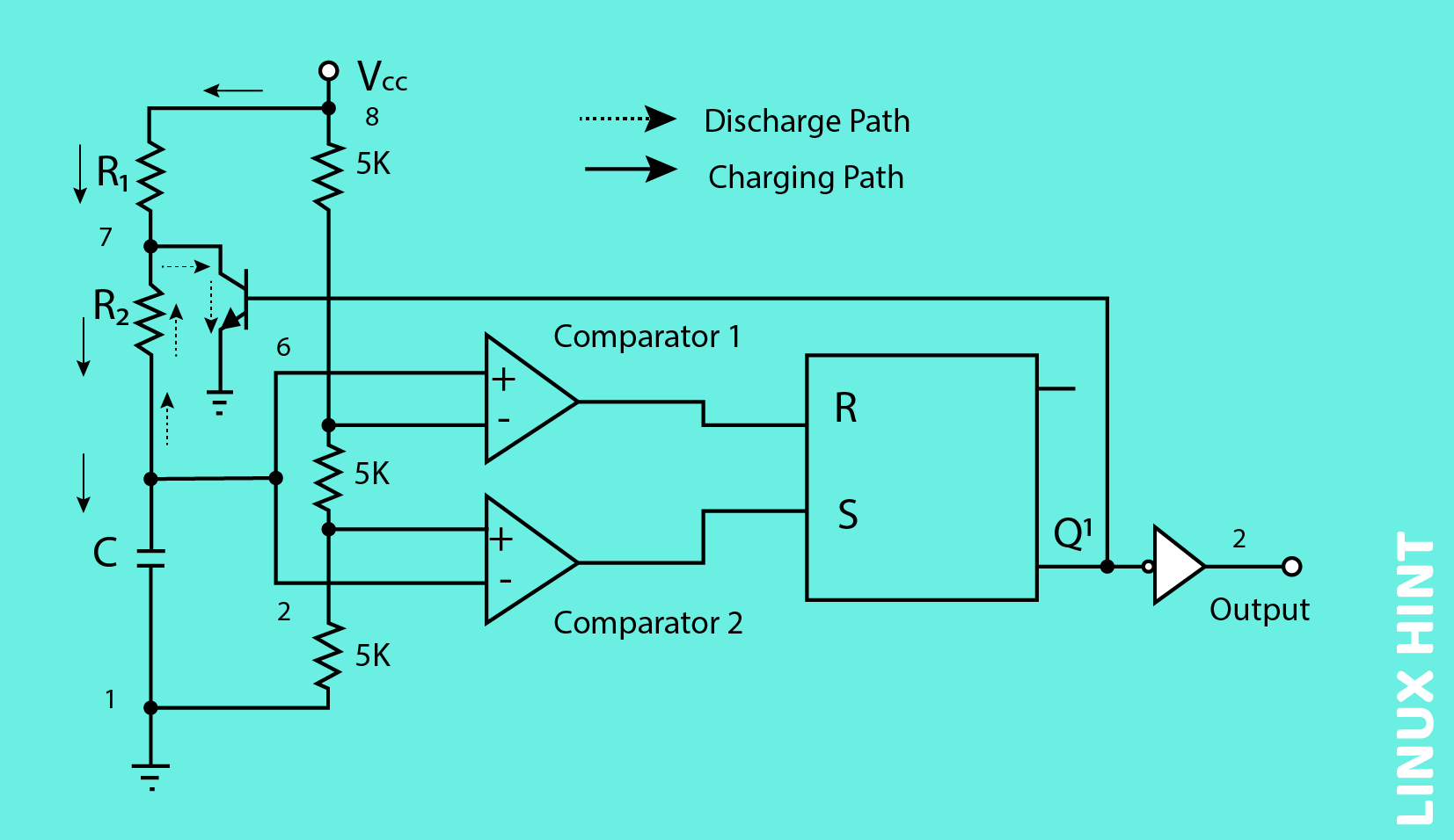
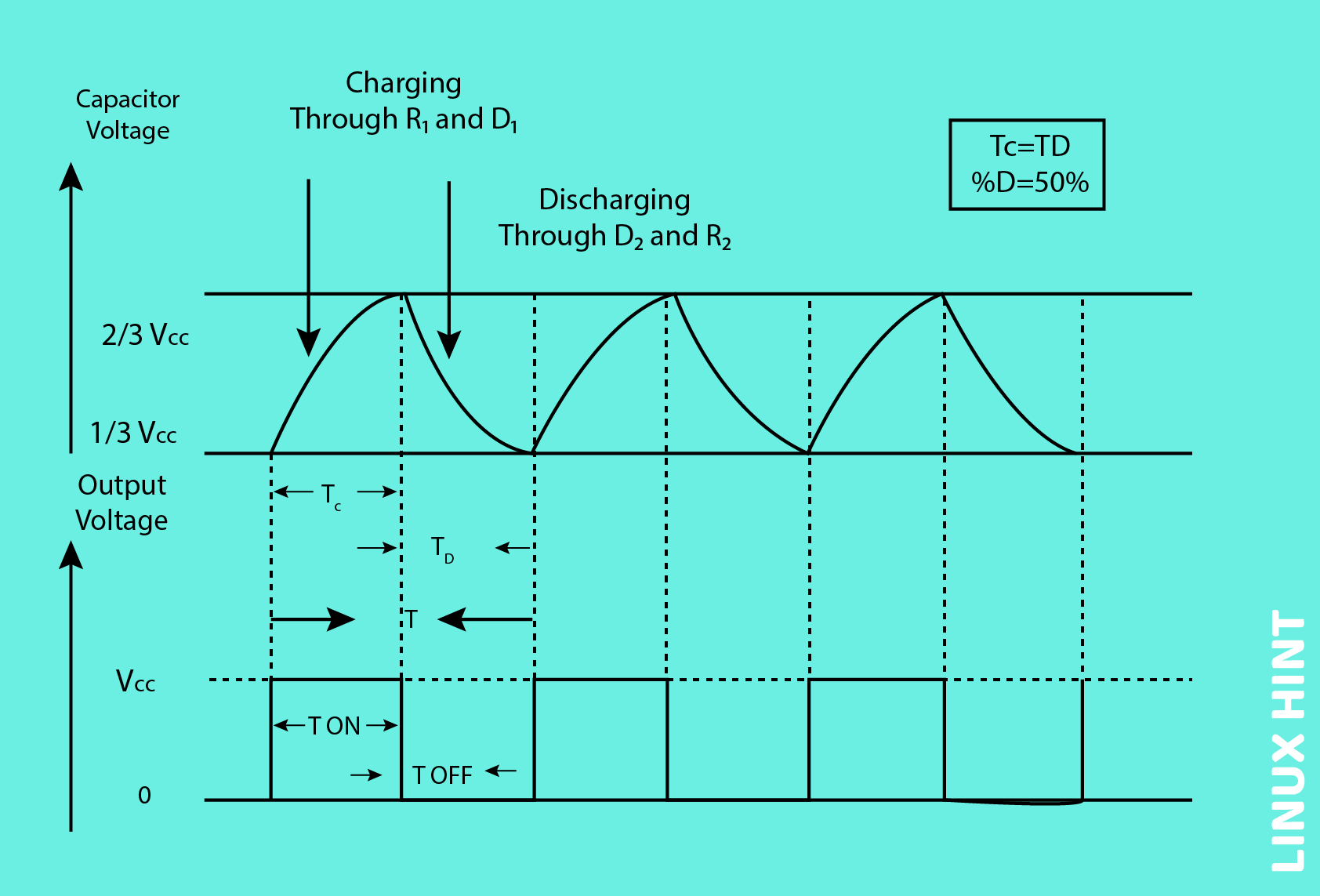
The flip-flop is first reset when connected with the supply, which causes the timer’s output to switch to a low state. As a result of being coupled to Q’, the discharge transistor is pushed to saturation point. The transistor will allow the timing circuit’s capacitor C, which is linked to Pin 7 of the IC 555, to discharge. The timer’s output is now negligible. The trigger voltage is the only voltage present across the capacitor in this case. As a result, if the capacitor voltage falls below 1/3 VCC, the reference voltage that activates comparator no. 2, the output of comparator no. 2 will become high during discharge. The flip-flop will be set as a result, producing a HIGH output for the timer at pin 3.
The transistor will be turned OFF by this high output. As a result, through resistors R1 and R2, the capacitor C charges up. Pin 6 is connected to the junction where the capacitor and resistor meet, therefore the voltage for the capacitor is now equal to the threshold voltage. As the capacitor charges, its voltage rises exponentially toward VCC; when it reaches 2/3 VCC, the threshold comparator’s reference voltage (comparator 1), its output spikes.
The flip-flop is hence RESET. The timer’s output decreases to LOW. This low output will restart the transistor, which gives the capacitor a discharge route. As a result, the resistor R2 will allow the capacitor C to discharge. Thus, the cycle keeps on.
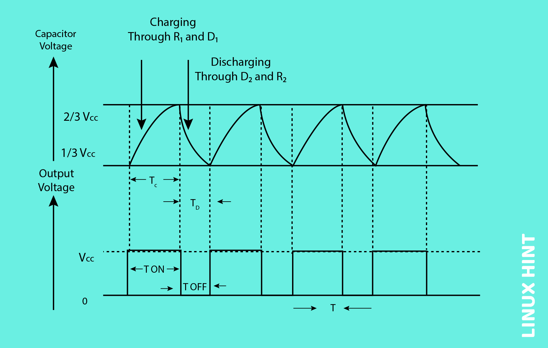
As a result, while the capacitor is charging, the output voltage is high at pin 3, and the voltage around the capacitor increases aggressively. Similar to this, pin 3’s output voltage is low, and as the capacitor discharges, its voltage across it falls off exponentially. The output waveform looks like a series of rectangular pulses.
Waveforms of Capacitor Voltage & Output Voltage
As a result, R1 + R2 represents the total resistance in the charging channel, and C represents the charging time constant. Only when the capacitor passes through the resistor R2 during discharge does it discharge. R2C is the discharge time constant as a result.
Duty Cycle
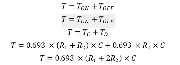
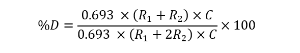
The resistances R1 and R2 affect the charging as well as the discharging time constants. The variation in the time constant is typically greater than the discharging time constant. The HIGH output continues to occur for a longer period than the LOW output as a result, and the output waveform is not symmetrical so If T is the duration of one cycle and TON is the time for higher output, then the duty cycle is given by:

So, the Duty Cycle in percentage will be:

Where T is the total of the charge and discharge times, TON and TOFF, the following equation provides the value of TON or the charge time TC:

The discharge time TD, often known as TOFF, is given by:

Consequently, the formula for the duration of one cycle T is:

Substituting in the formula of % Duty Cycle:

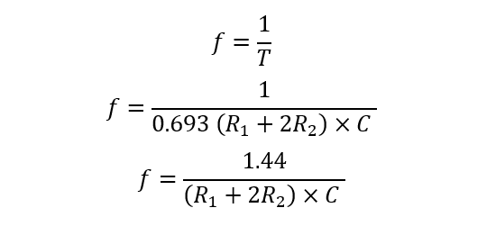
Frequency is given by:
Application – Generation of Square Waves
An astable multivibrator’s duty cycle is usually higher than 50%. When the duty cycle is precisely 50%, an astable multivibrator produces a square wave as its output. Duty cycles of 50% or anything lower than that are difficult to achieve with the IC 555 acting as an astable multivibrator, as was previously mentioned. The circuit has to go through some changes.
Two diodes are added, one in parallel with resistor R2 and the other in series with resistor R2 with the cathode connected to the capacitor. By changing the resistors R1 and R2, it is possible to create a duty cycle in the bracket of 5% to 95%. The circuit for creating square waves output can be configured as below:
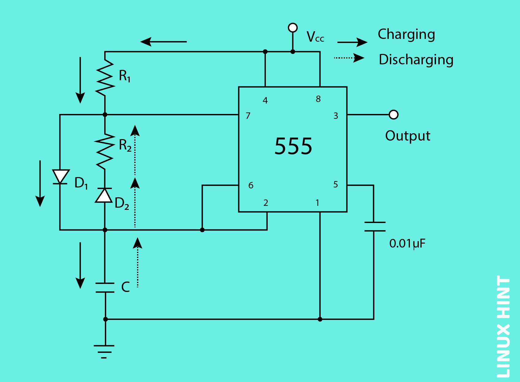
In this circuit, the capacitor charges while transferring current via R1, D1, and R2 during charging. It discharges via D2 and R2 when discharging.
The charging time constant, TON = TC, may be calculated as follows:

And this is how you get the discharge time constant, TOFF = TD:

Consequently, the duty cycle D is determined by:

Making R1 and R2 equal in value will result in a square wave with a 50% duty cycle.
A duty cycle of less than 50% is reached when R1’s resistance is lower than R2’s while normally R1 and R2 may be replaced by potentiometers to accomplish this. Without utilizing any diodes, another square wave generator circuit may be built using an astable multivibrator. R2 is connected between pins 3 and 2, or the output terminal and the trigger terminal. Below is a diagram of the circuit:
Both charging and discharging processes in this circuit take place only via resistor R2. The capacitor should not be exposed to outside connections when charging by the resistor R1, which should be set at a high value. Additionally, it serves to guarantee that the capacitor charges to its full potential (VCC).
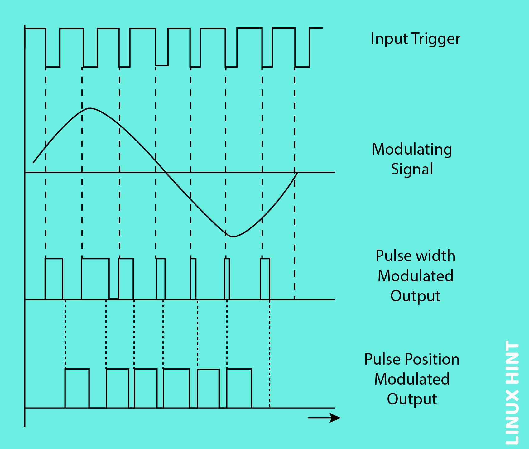
Application – Pulse Position Variations
Two 555 timer ICs, one of which runs in astable mode and the contrary in monostable mode, offer pulse position modulation. First, IC 555 is in astable mode, the modulation signal applies at Pin 5 and the IC 555 produces a pulse-width modulated wave as its output. The triggering input of the next IC 555, which is running in monostable mode, receives this PWM signal. The location of the second IC 555’s output pulses vary by the PWM signal, which is once again reliant on the modulating signal.
Below is the circuit configuration for a pulse position modulator that uses two 555 timer integrated circuits.
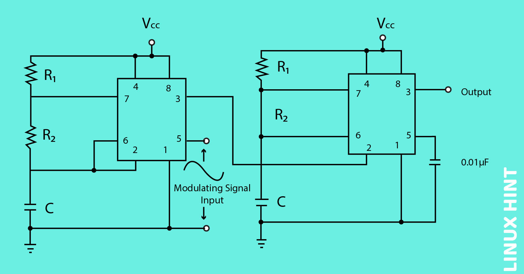
The control voltage, which determines the minimum voltage or threshold level for the first IC 555, is adjusted to create the UTL (Upper Threshold Level).

As the threshold voltage changes in relation to the modulating signal being applied, the pulse width and time delay change as well. When this PWM signal is applied to trigger the second IC, the only thing that will change is the location of the output pulse, neither its amplitude nor breadth will change.
Conclusion
The 555 Timer ICs can function as a free-running oscillator or an astable multivibrator when combined with additional components. 555 Timer ICs in astable mode are used in a wide variety of applications ranging from pulse train generation, modulation, and square wave generations.