Binary adders are basically arithmetic adder circuits. These circuits are made by combining AND gates with XOR gates in basic configuration. They can also combine OR gates in advanced configurations. This article discusses binary adders in detail.
Binary Adder
Any digital computer must be able to execute the two fundamental mathematical operations of addition and subtraction. The four fundamental binary two-bit addition operations are shown below.
Each of the first three operations, binary addition, results in a total of one bit, either a 0 or a 1. However, the outcome of the fourth addition operation, which uses the inputs 1 and 1, is two binary numbers. Here, the higher of the significant bit is referred to as the Carry, while the lower of the significant bit is referred to as the Sum.
There are no limitations in addition to a single bit. When we attempt to combine binary integers with more than one bit, a limitation occurs.
The term “Binary Adder Circuits” refers to logic circuits that are created to add two binary integers. They are categorized into the following categories according on how they handle the result of the addition “1+1”, which are:
These are discussed further in detail below.
Half Adder
A Half Adder circuit is a kind of logic device used to add two 1-bit values, or simply two bits. There are two inputs and outputs in this circuit. The two 1-bit binary values Augend and Addend are the inputs, while outputs are sum and carry.
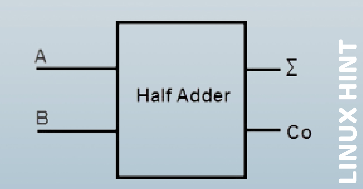
Block Diagram
The block diagram for Half Adder may be seen in the figure below:
Truth Table
The Truth table for half adder is provided below:
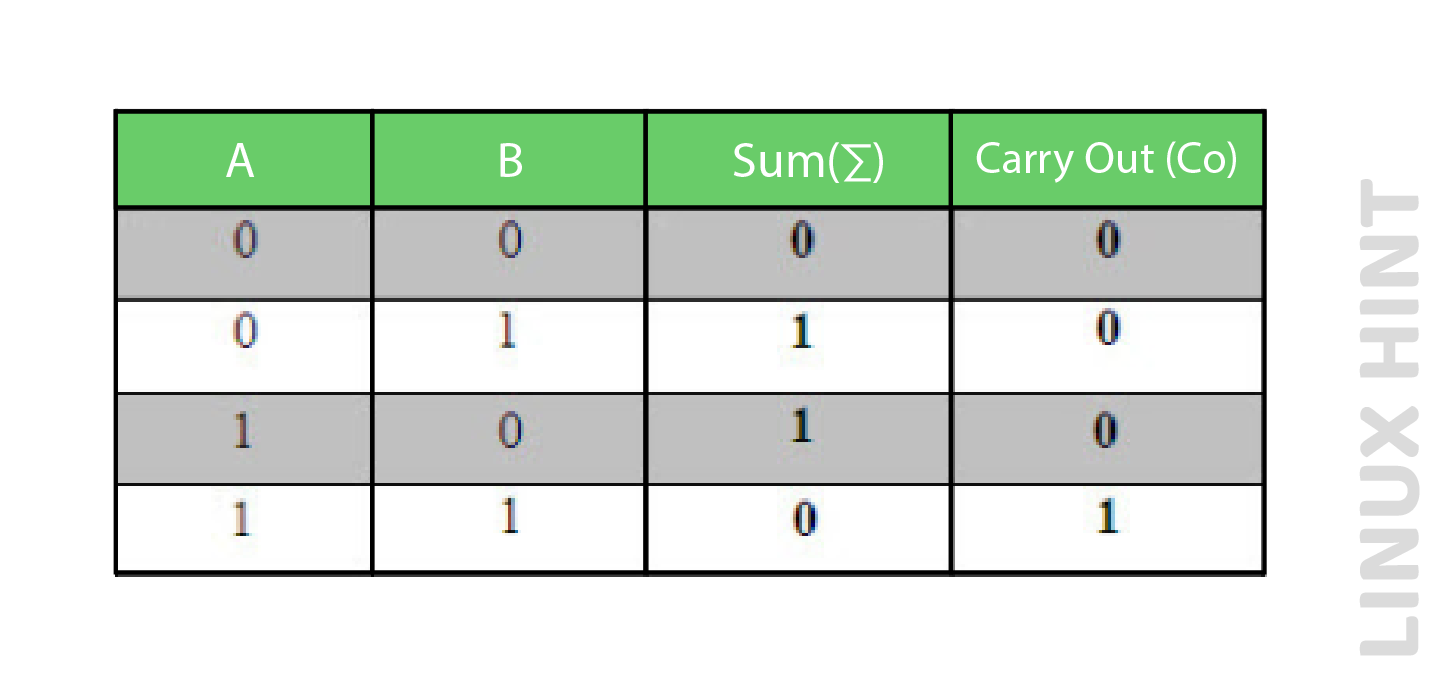
It seems like an Ex-OR gate if we look at the ‘Sum’ values in the truth table.
Therefore, an AND gate for the carry output and an XOR gate for the sum output are required for a suitable implementation of a half adder. The logic diagram for a half adder may be seen in the figure below:
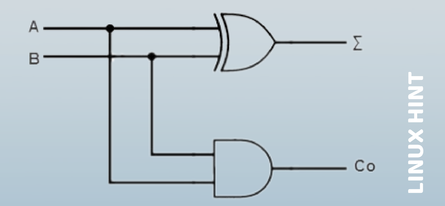
The inputs of the half-adder circuit above are designated as A and B. The carry output is marked with CO, while the ‘Sum’ output is marked with the summation symbol ().
First order binary numbers, or 1-bit binary numbers, are added and added to using half adders. Binary numbers with multiple bits cannot be added in half adder. This is because the half adder cannot cater for the ‘carry’ input from the previous sum.
Full Adder
Combinational logic circuit known as a full adder adds three bits and generates two outputs comprising sum output and carry output. The full adder is used to add three numbers at once since, as we have seen, the half adder is unable to handle three inputs.
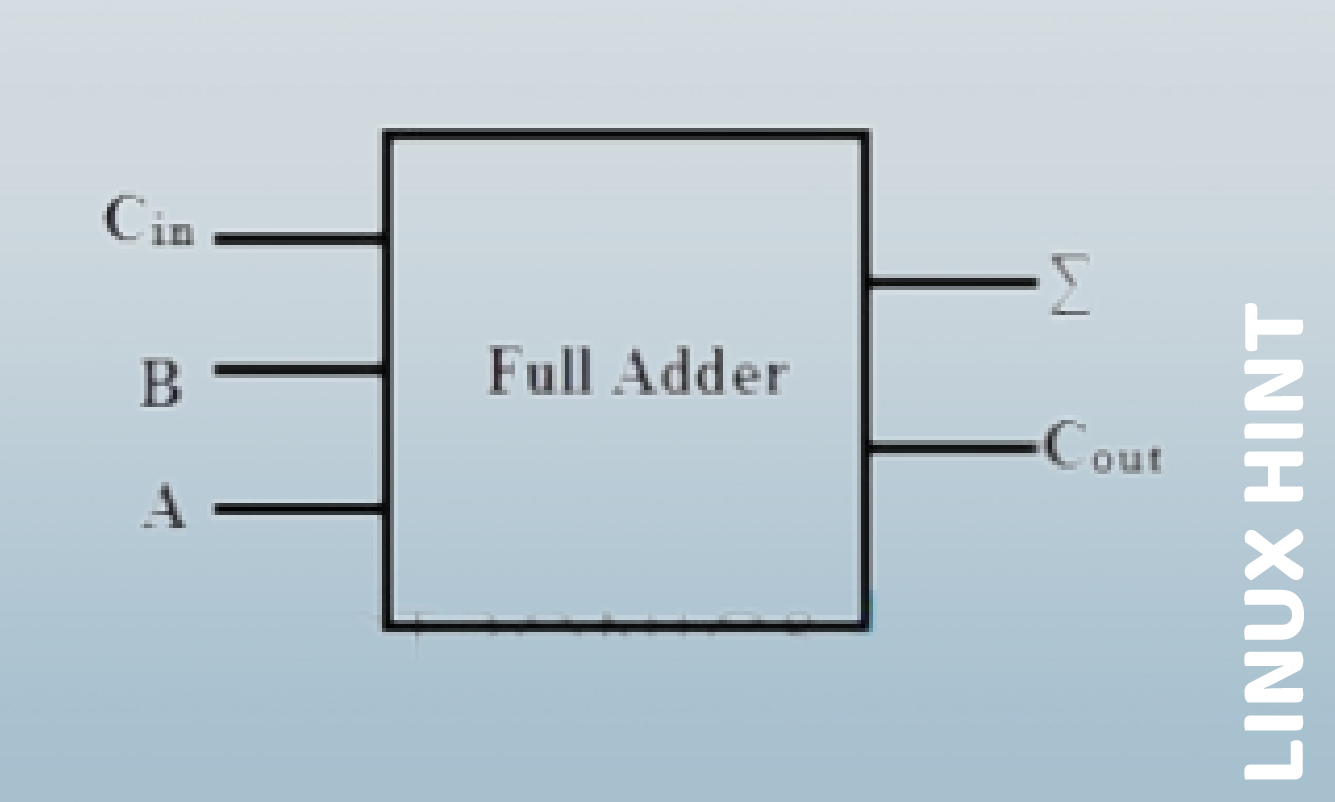
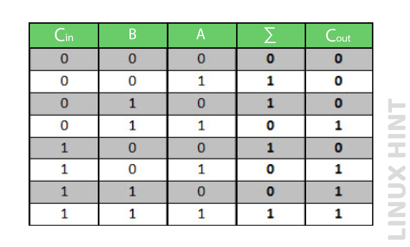
It has three inputs: the carry from the previous addition is the third input terminal, and the first two inputs indicate the addition for the two significant bits.
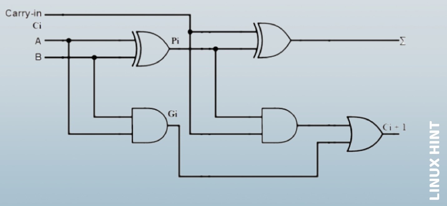
A, B, and CIN are used to identify the inputs in the below diagram of a full adder, while and COUT are used to identify the outputs.
Truth table
Circuit Diagram
A full adder may also be created by combining two numbers of half adders with a single OR Gate.
The full adder circuit shown below uses two half adders with an OR gate. Here, the inputs are A and B, the carry input is CIN while the carry and sum outputs are COUT.
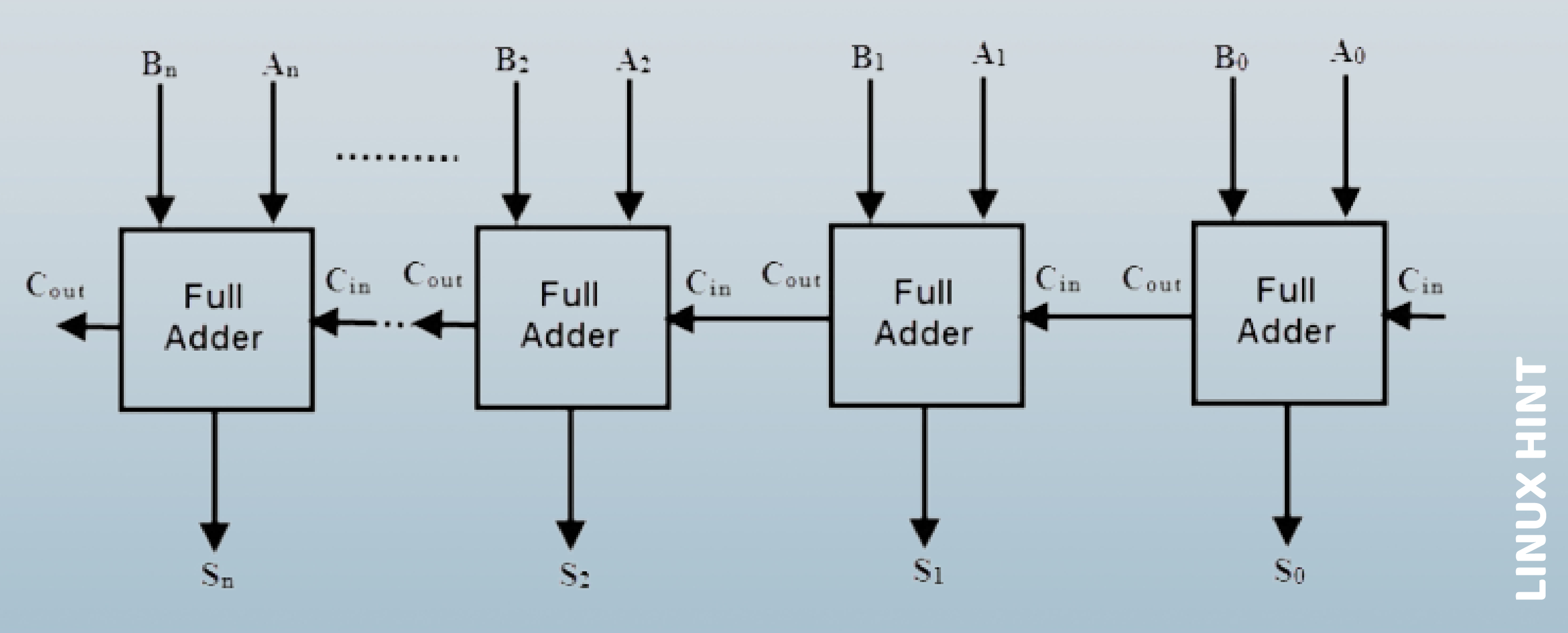
N-Bit Parallel Full Adder
A single full adder can handle both the carry input and the addition of two one-bit values. Multiple full adders are needed to conduct the addition of binary integers containing multiple bits, and the number of full adders needed depends on the bits number. A parallel adder, which adds all the bits of the two integers concurrently, is hence a combination of multiple full adders.
An n-bit parallel adder may be built by connecting ‘n’ complete adders in parallel. Given that there is no carry in the least significant position of the following figure, we may either use a half adder or set the carry input of a full adder to zero at this location.
4-Bit Parallel Full Adder
A parallel 4-bit binary adder with three numbers of full adders and one-half adder is shown in the accompanying image. ‘A3 A2 A1 A0’ and ‘B3 B2 B1 B0’ are the two binary integers that need to be added, and they are applied to the appropriate inputs of the Full Adders. The output of this parallel adder is “C4 S3 S2 S1 S0”, where C4 denotes the last carry.
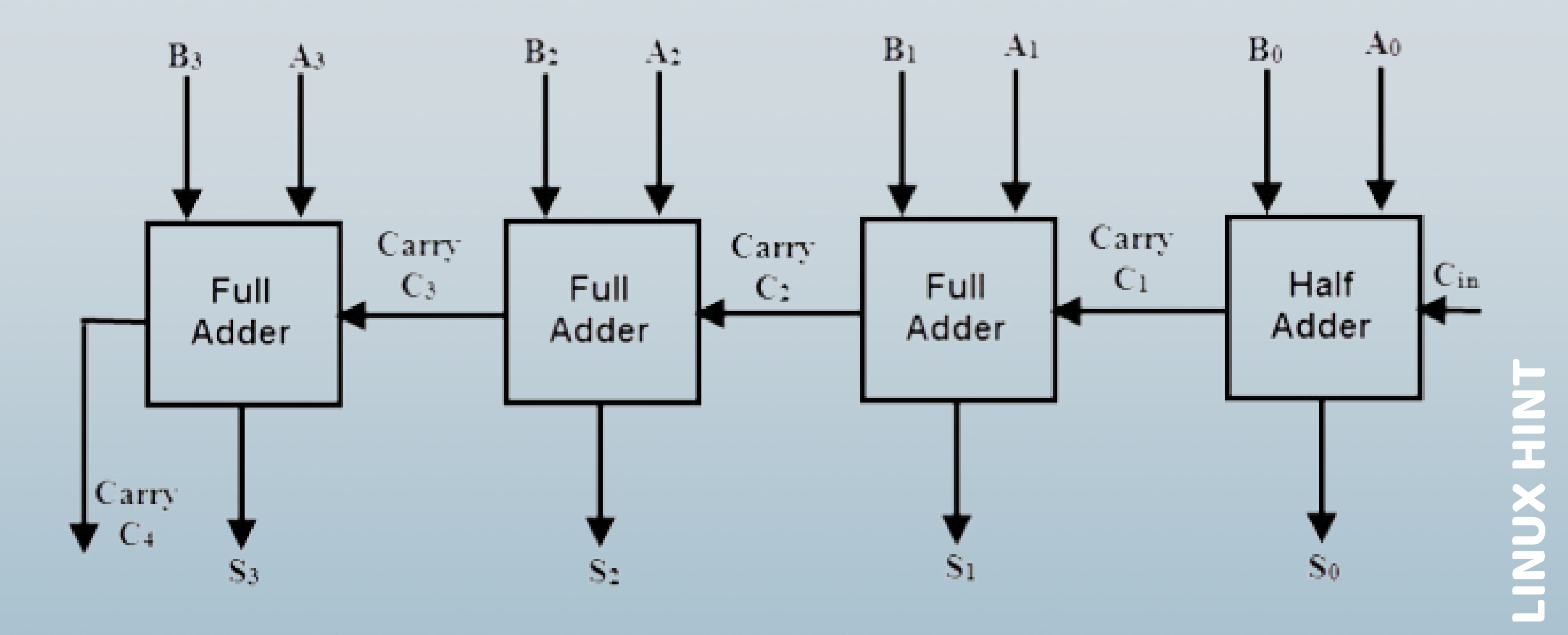
The first segment of the four-bit adder is a half-adder, which takes two of the inputs as A0 and B0 and outputs a sum and a carry bit. The input Carry C0 for the first segment, which may also be a complete adder, must be zero.
Given that the next three blocks have three numbers of inputs (two numbers of the main binary bits and one number of the carry bit from the previous step), they should be complete adders. As a result, the second block complete adder generates the values S1 and C2. The other two complete adders will come after this, and the end result is C4 S3 S2 S1 S0.
Full adders are often created as twin in-line packaging integrated circuits. A well-liked 4-bit full adder IC is the 74LS283. These parallel adders are part of the arithmetic and logic Unit, or ALU, of a unit computer and are used to add binary values.
Conclusion
Binary addition is achieved through half adders and full adders. In case of multiple bits, full adders are used as half adders are unable to handle multiple bits for addition. Half adders are made from combination of AND gate with XOR gate while full adder is made from combination of two half adders with OR gate.