Junction Field Effect Transistors
Junction Field Effect Transistors are voltage-controlled semiconductor-based transistors. These are unidirectional transistors with three terminals; drain, source and gate. JFETs do not have PN junctions, but they are composed of channels of semiconductor materials.
Construction & Classifications
JFETs have a large channel for flow of majority charge carriers. This channel is known as substrate. The substrate can be of P-type or N-type material. Two external contacts known as ohmic contacts are placed across the two ends of the channel. JFETs are classified based on the semiconductor material of substrate in their construction.
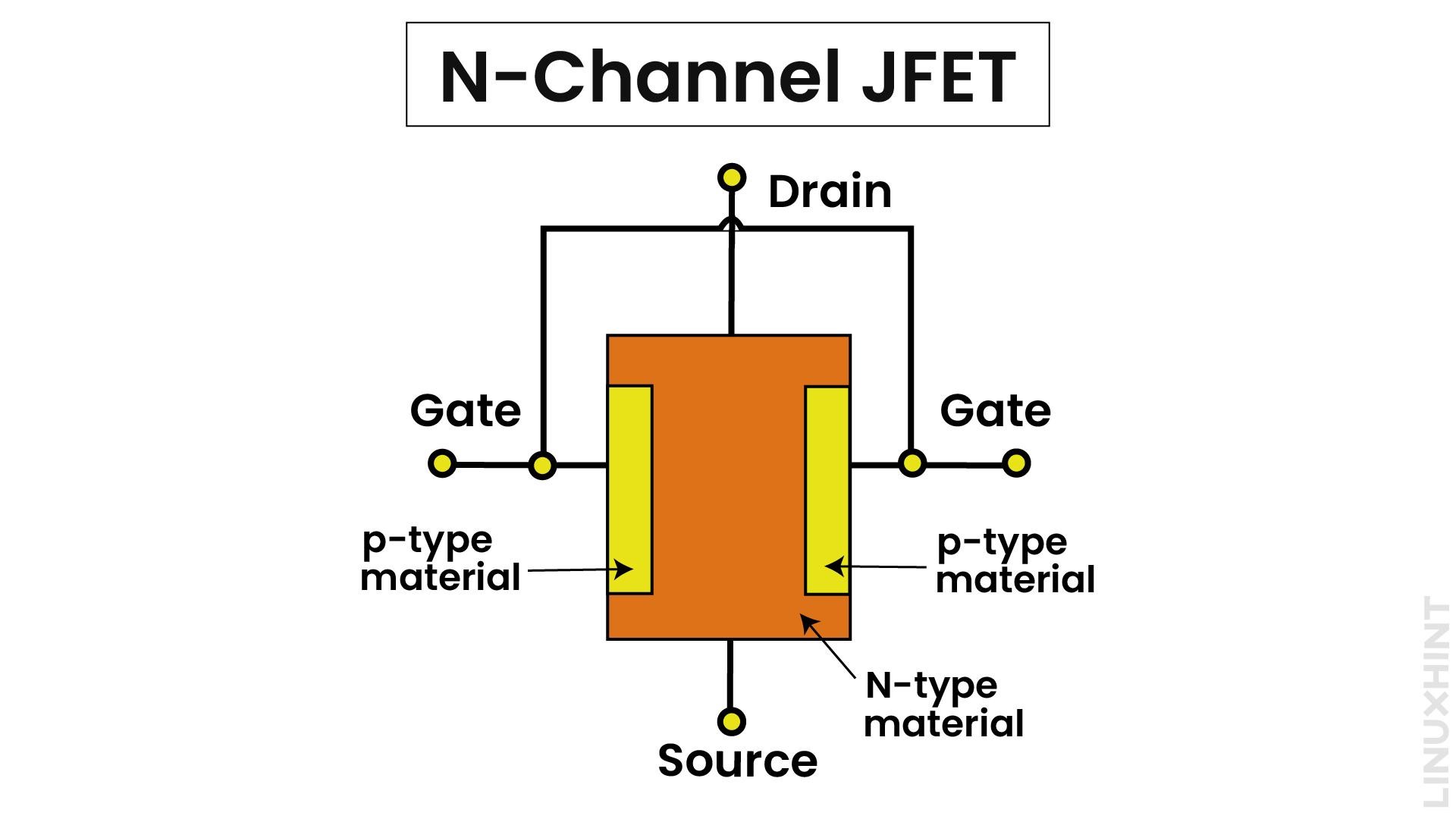
N-Channel JFET Transistors
The channel is made from N-type impurity material, while gates are composed of P-type impurity material. N-type material means the pentavalent impurities have been doped, and the majority charge carriers are free electrons in the channel. The basic construction and symbolic presentation of N-Channel JFETs is shown below:
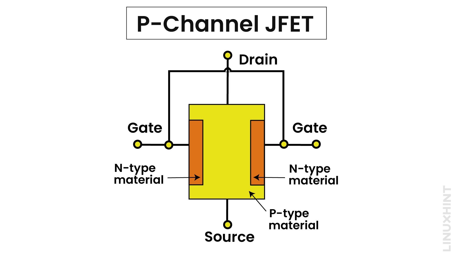
P-Channel JFET Transistors
The channel is composed of P-type impurity material while gates are composed of N-type impurity material. P-Channel means that trivalent impurities have been doped in the channel and majority charge carriers are holes. The basic construction and symbolic presentation of P-Channel JFET is shown below:
Working of JFETs
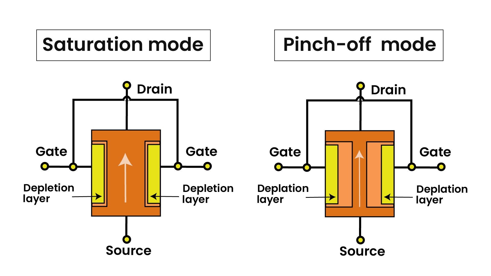
JFETs are often described with analogy of water hose pipe. The flow of water through pipes is analogous with the flow of electrons through channels of JFETs. The squeezing of the water pipe decides the amount of flow of water. Similarly, in the case of JFETs, the application of voltages across gate terminals decides the narrowing or widening of the channel for movement of charges from source to drain.
When reverse bias voltage across gate and source is applied, the channel narrows while depletion layer increases. This mode of operation is called pinch-off mode. This kind of channel behavior is represented below:
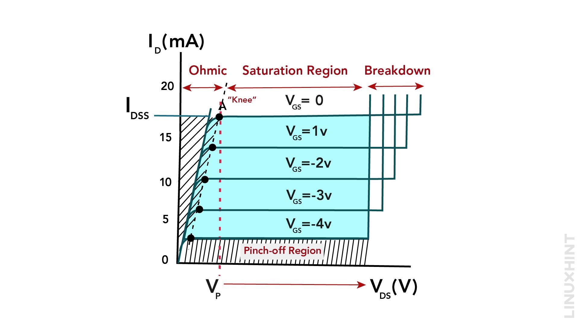
JFET Characteristics Curve
JFETs are depletion mode devices, which means that they operate on widening or narrowing of depletion layers. To analyze the complete operation modes, the following biasing arrangement is applied across an N-Channel JFET.
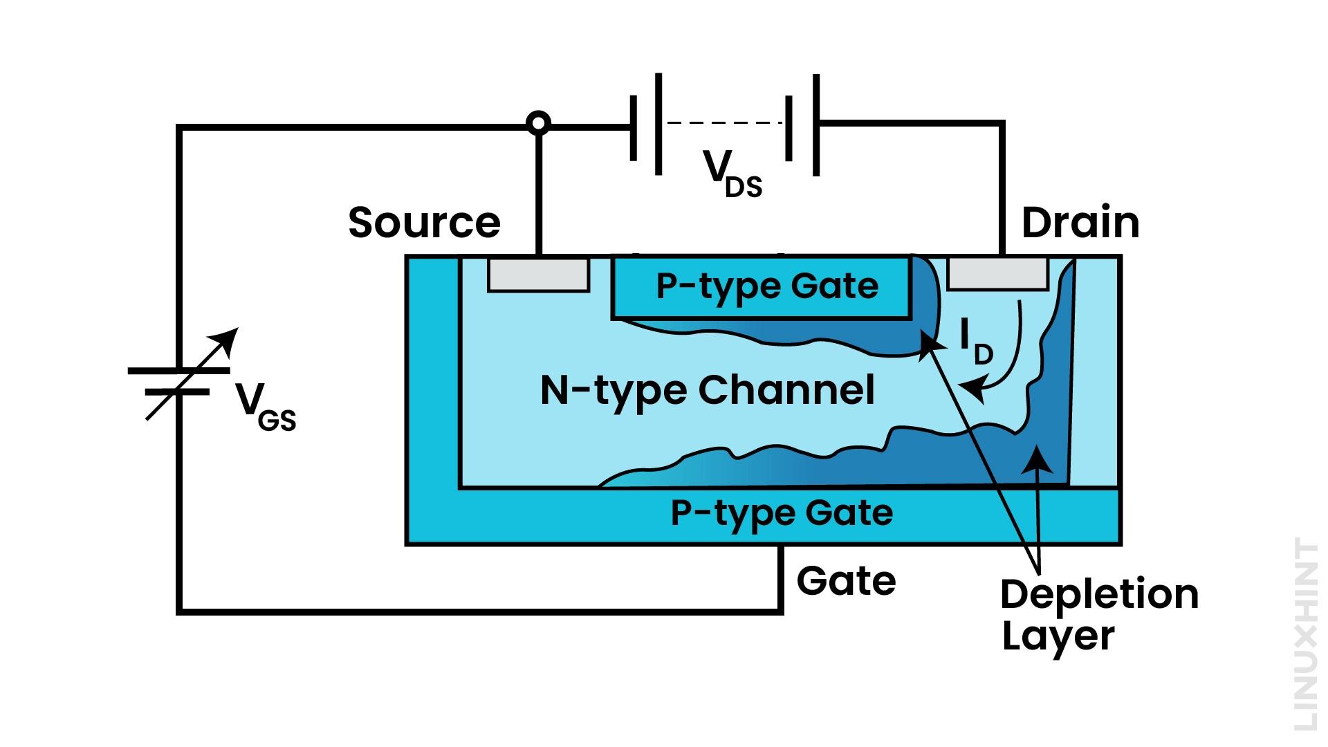
Two different biasing voltages are applied at JFET terminals. VDS is applied between drain and source while VGS is applied between gate and source as shown in above figure.
JFET shall operate in four different modes of operation, as discussed below.
1: Ohmic Mode
Ohmic mode is a normal state without any biasing voltages applied across its terminals. Therefore, VGS=0 in ohmic mode. The depletion layer shall be very thin and JFET operates like an ohmic element such as a resistor.
2: Pinch-Off Mode
In cut-off mode, sufficient biasing voltage across the gate and source is applied. The applied reverse bias voltage stretches the depletion region to maximum level and therefore the channel behaves like an open switch resisting the flow of current.
3: Saturation Mode
The gate and source bias voltage controls the current flow across the channel of JFET. The current varies with change in biasing voltage. The drain and source bias voltage has negligible effect in this mode.
4: Breakdown Mode
The drain and source bias voltage increases to a level that breaks down the depletion layer in the channel of JFETs. This leads to maximum current flow across the channel.
Mathematical Expressions for JFETs Parameters
In saturation modes, the JFETs enter conductor modes where voltage varies the current. Therefore, the drain current can be evaluated. The expression for evaluating drain current is given by:

The channel widens or narrows with application of gate voltages. The resistance of channel with respect to application of drain-source voltage is expressed as:

RDS can also be calculated through transconductance gain, gm:

JFET’s Configurations
JFETs can be connected in a variety of ways with the input voltages. These configurations are known as common source, common gate and common drain configurations.
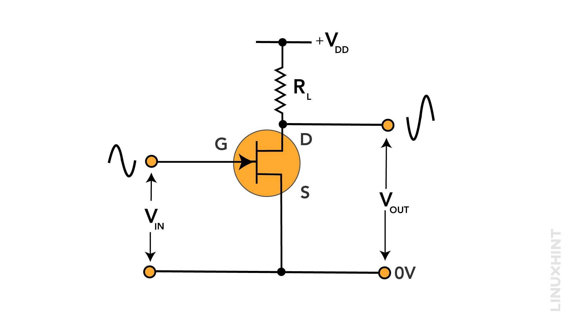
Common Source Configuration
In common source configuration, the source of JFET is grounded and input is connected to the gate terminal while output is taken from the drain. This configuration offers high input impedance and voltage amplification functions. This amplifier mode configuration is the most common of all JFETs configurations. The output obtained is 180 degrees out of phase with input.
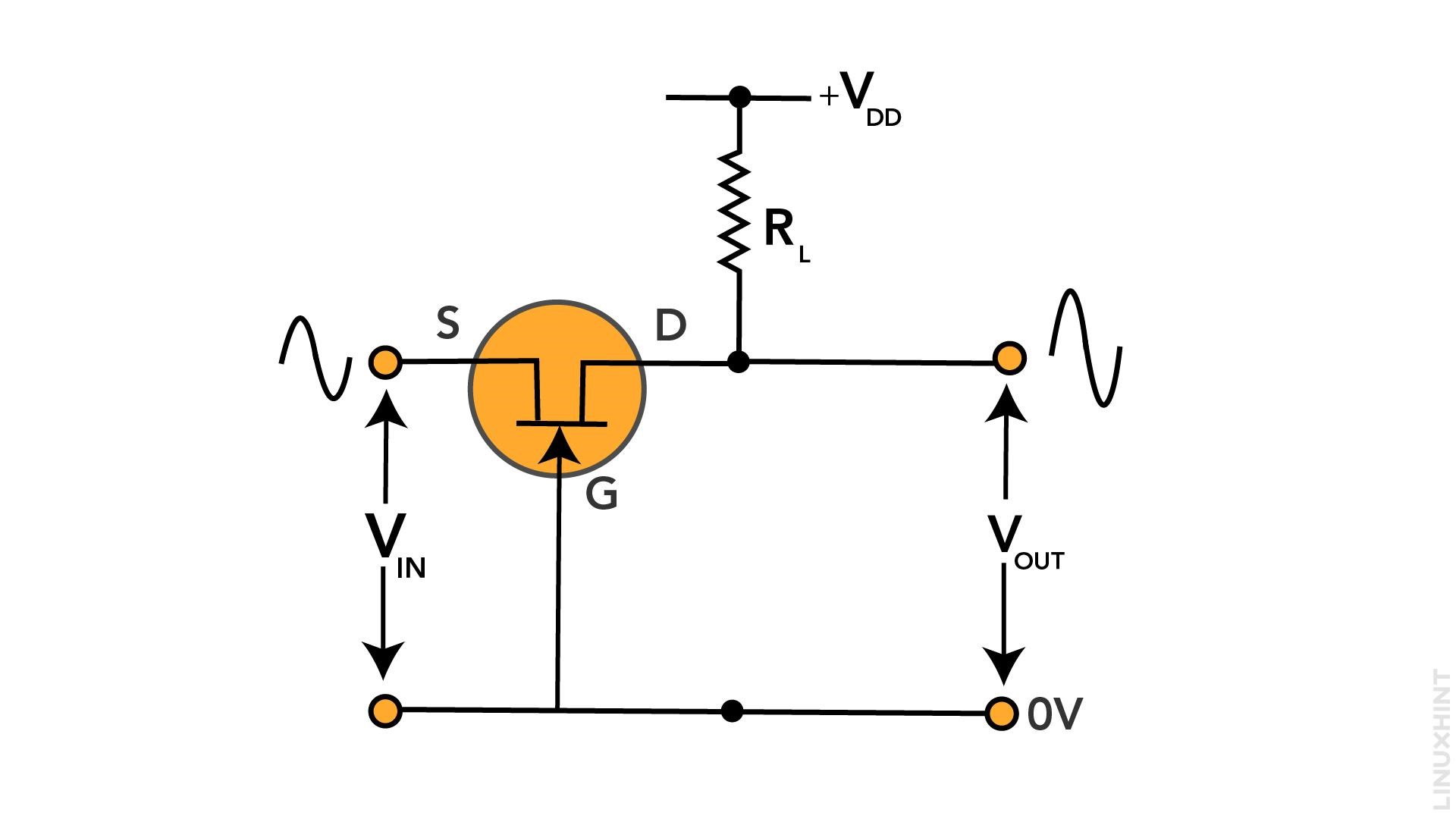
Common Gate Configuration
In a common gate configuration, the gate is grounded while input is connected to source and output is taken from drain. As the gate is connected with ground, the configuration has low input impedance but higher impedance at output. The output obtained is in phase with input:
Common Drain Configuration
In a common drain, input is connected to the gate while output is connected from the source terminal. This configuration also offers low input impedance and higher output impedance just like common gate configuration, but the voltage gain is approximately unity here.
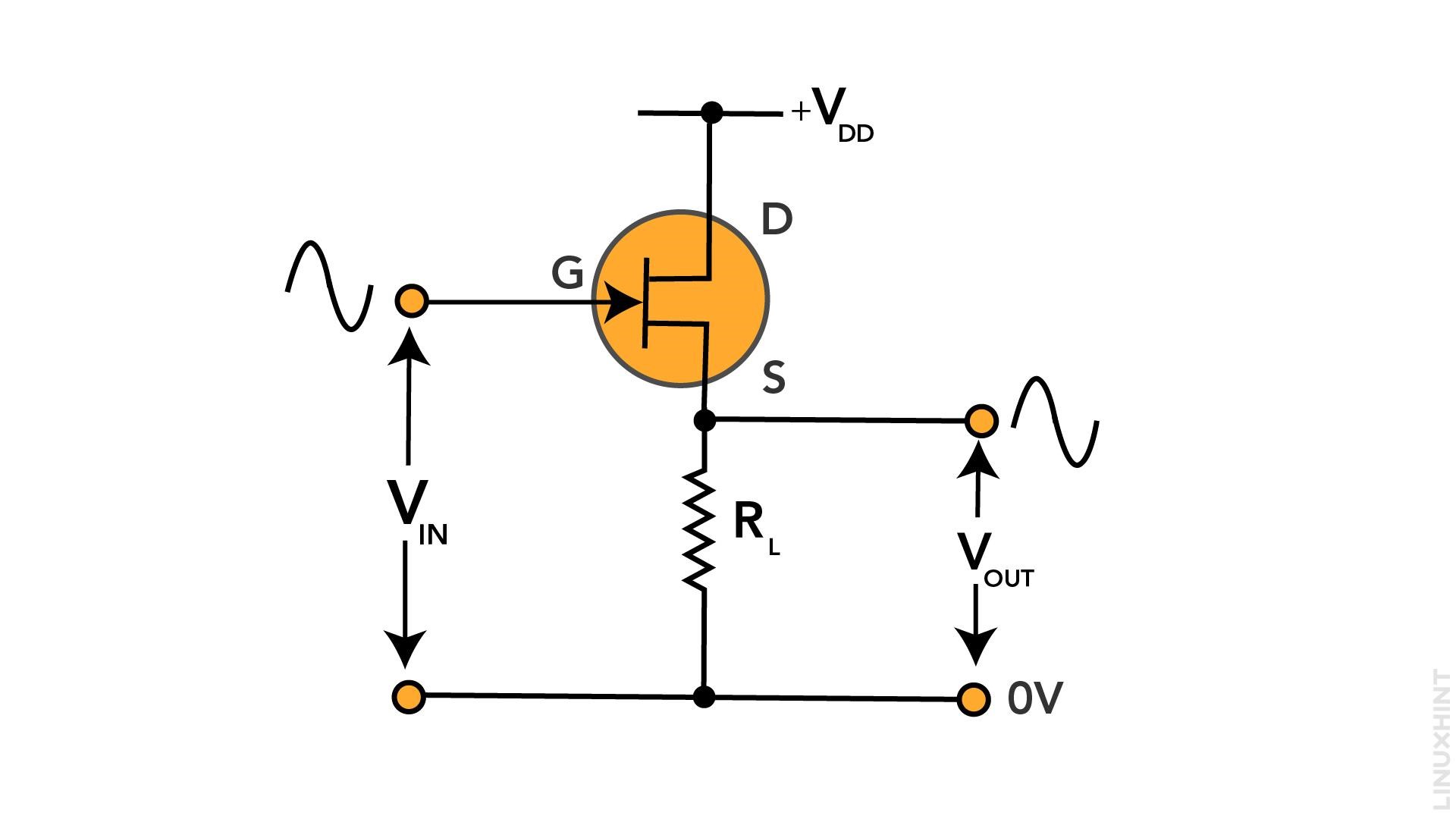
This configuration also matches with common source where input is connected to gate, but common source configuration has gain less than unity.
Application – JFETs Amplifier Configuration
JFETs can be made to work as Class-A amplifiers when the gate terminal is connected with a voltage divider network. An external voltage is applied across the source terminal, which is mostly configured to be one-fourth of VDD in the below circuit.
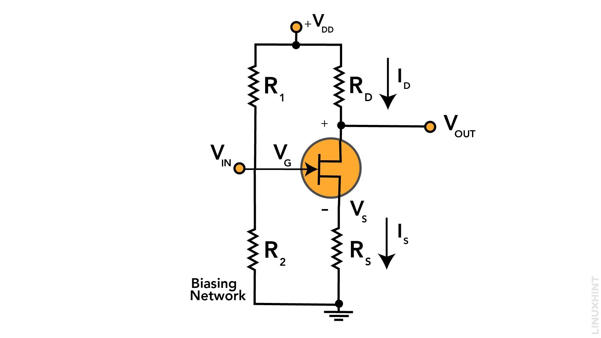
The source voltage can therefore be expressed as:

Also, source voltage can be calculated through below expression:

The drain current can be calculated from above configuration as below:

The gate voltage can be obtained as a function of the values of resistors R1 & R2 as provided below.

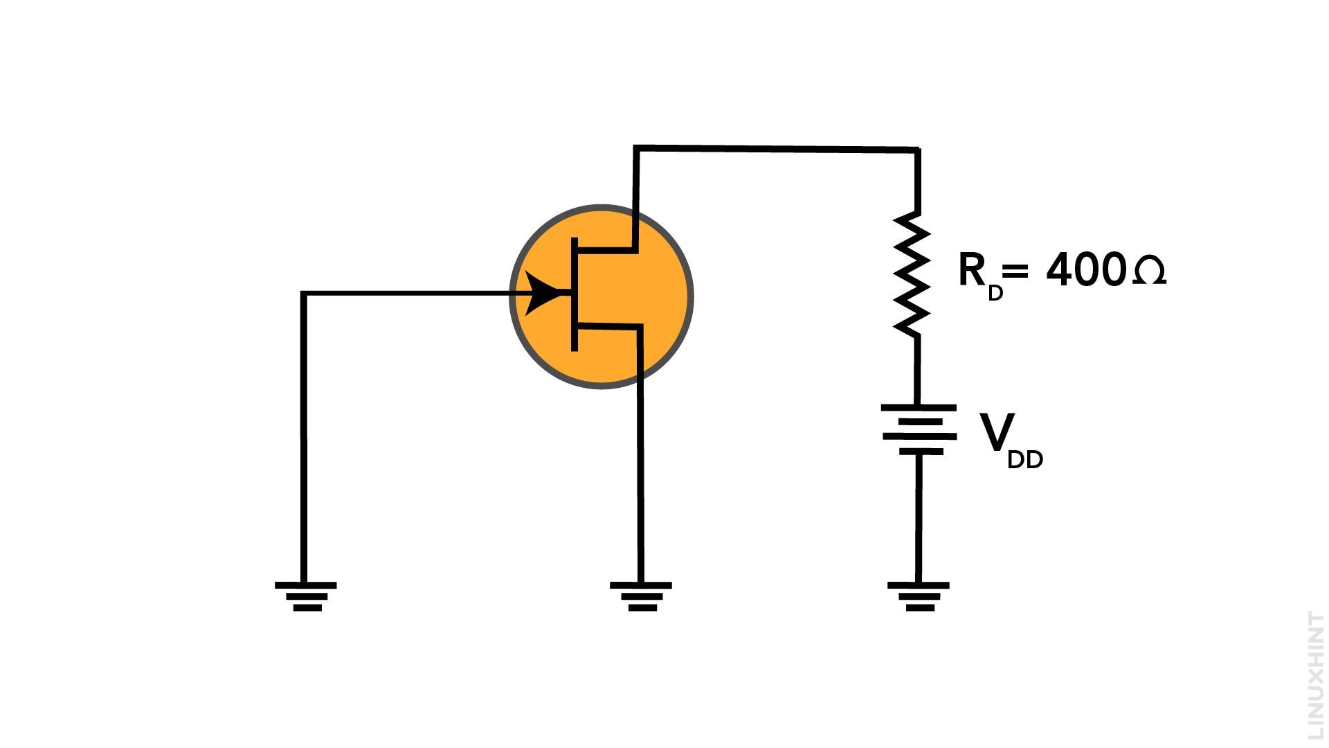
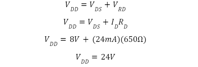
Example 1: Calculating VDD
If VGS(off)=-8V, IDSS=24mA for JFET in below configuration, calculate VDD as shown in figure when RD=400.
Since
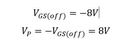
The above shall be the minimum value of VDS for JFET to operate in constant current region, therefore:

Also,

By applying KVL at drain circuit:

Example 2: Determine the Value of Drain Current
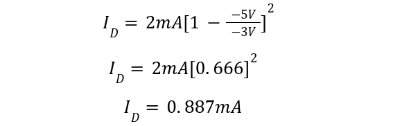
Determine the value of drain current when VGS=3V, VGS(Off)=-5V, IDSS=2mA for below JFET configuration.

The expression for drain current is:

Conclusion
Junction Field Effect Transistors are three terminal semiconductor devices that work with behavior of the depletion regions in different modes of operation. They do not have PN junctions, but they are made of channels of semiconductor materials.