The shape and structure of semiconductor symbols give an idea about their functionality and also tell us the direction of current flow. These symbols also help us to properly connect the semiconductor devices in an electrical circuit by looking at their appropriate electrical polarities. One main thing one must know is that these symbols do not exactly describe the physical device. The physical arrangement of semiconductor devices in an electrical circuit board is different from the symbolic representation in a circuit diagram.
Electrical circuit diagrams contain multiple different graphical symbols. Previously, these symbol’s representations were different for each country. But in recent times, we have seen different changes that are made to standardize semiconductor symbols internationally. Especially the frequently used symbols like diodes, transistors, and power electronic devices will now share a common design. The semiconductor symbols discussed in this article are according to the recommendations of both the International Electrotechnical Commission (IEC) and the British Standards Institution (BSI).
Quick Outline:
- Schematic Semiconductor Symbols for Diodes
- Schematic Semiconductor Symbols for Bipolar Junction Transistors
- Schematic Symbols for FET (Field Effect Transistors)
- Schematic Semiconductor Symbols for Power Devices
- Conclusion
Schematic Semiconductor Symbols for Diodes
Semiconductor diodes have different types, with each type having a unique schematic symbol. Mainly these types of diodes include the symbol of pn-junction diode, Schottky diode, photodiode, and light-emitting diode (LED). The basic structure of their symbol and schematic is pretty much similar to a basic diode. The only difference is in their input and output terminals. As each of these symbols represents a completely different diode with distinct functioning.
A diode is a simple two-terminal device that is designed using two semiconductor materials. These two types of material are N-type and P-type. To create a pn-junction the n-type material acts as the cathode and the p-type material acts as the anode. In semiconductors, schematic symbols help to identify the difference between the anode and cathode. The anode is represented by the letter A and the cathode of the diode is denoted by the letter K. In some schematics, you will also see a color lead for the cathode terminal.
The diode schematic symbol has an arrowhead. This arrow is pointed from Anode (A) to Cathode (K). This arrow direction also describes the direction of conventional current flow when the diode is in forward-biased condition. However, if the voltage polarity of the diode is reversed, there will be no current flow.
Schematic symbols for Zener diodes and Schottky diodes are similar to the symbol of a basic pn-junction diode. It has one difference, which is a bent line that represents the Cathode (K) terminal. On the other hand, the schematic symbol for a light-emitting diode (LED) has smaller arrows radiating from it when the diode is in forward-biased condition. This represents that the light energy is being emitted by the light-emitting diode.
| Schematic Symbol | Symbol Name | Description |
|---|---|---|
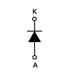 |
Semiconductor Diode | It is a type of diode with pn-junction that can conduct current when the diode is forward-biased. It blocks the current in the reverse-biased state. These are used in small-signal circuits, rectification processes, and high-current applications. |
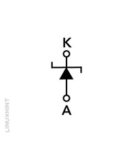 |
Zener Diode | This type of diode operates in its reverse-voltage breakdown region. You can use this diode for voltage limiting, transient suppression, and regulation of circuits. You can find this diode type available in various reverse breakdown voltage values. |
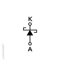 |
Schottky Diode | This type of diode contains an n-type semiconductor. It also has a metal electrode junction. It has a low forward voltage drop compared to the pn-junction diodes. Further, it also has minimal power dissipation, and it also has a faster switching rate when compared with pn-junction diodes. |
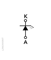 |
Light-emitting diode (LED) | This is a semiconductor diode that operates in forward-biased states. It can emit visible and non-visible colored light when it is in a forward-biased state. The amount of light that is emitted by this diode is dependent on the materials and doping used. |
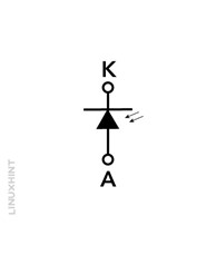 |
Photodiode | It is a semiconductor photo sensor diode. When light is incident on this diode, current starts to flow in the reverse direction. |
Schematic Semiconductor Symbols for Bipolar Junction Transistors
Bipolar junction transistors (BJTs) have schematic symbols that represent the two main types of transistors: NPN (Negative-Positive-Negative) and PNP (Positive-Negative-Positive). If you see a circle around the bipolar transistor schematic symbol, it means it is a standalone device. On the other hand, if the symbol is without any circle, it indicates its use within internal circuitry, such as logic gates and digital ICs.
BJTs have three terminals marked as C (Collector), B (Base), and the last terminal E (Emitter). Current in the BJTs flows from the Emitter side to the Collector, and the Base of the BJTs controls this flow of current. Most of the time you will not see these symbols on circuit diagrams, but these letters are added for more clarity.
There are some other specialized BJTs, like Darlington transistors and phototransistors. Darlington transistors combine the two transistors into one device. While the phototransistors use light energy in place of the Base terminal to operate.
| Schematic Symbol | Symbol Name | Description |
|---|---|---|
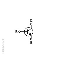 |
NPN Bipolar Transistor | An NPN bipolar transistor has a lightly doped p-type base region. This p-type base region is between the n-type emitter and collector regions of the bipolar transistor. The arrow on the symbol represents the conventional current flow direction. This current is flowing out of the transistor. |
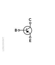 |
PNP Bipolar Transistor | The PNP transistor has a lightly doped n-type base region between the two p-type emitter and collector regions. The arrow represents the conventional current direction. In PNP, the current is flowing into the transistor. |
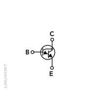 |
Darlington Pair Transistor | This type of transistor has two NPN or PNP bipolar transistors that are connected in series with a common collector configuration. This configuration will increase the overall current gain. This type of transistor is available in both PNP and Sziklai pair configurations. |
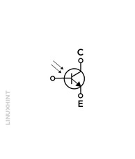 |
Phototransistor | An NPN phototransistor is enclosed in a protective case with a glass lens or window. It is used for detecting visible and near-infrared light sources from the environment. Some of its models include a base (B) lead for biasing and sensitivity control. |
Schematic Symbols for FET (Field Effect Transistors)
Field Effect Transistors (FETs) are three-terminal devices that have a wide range of different types. Each of its types has its own semiconductor symbol that can describe its operational characteristics. Different labels are used for the symbolic representations of field effect transistors. These labels include the letters D, G, and S to denote their respective terminals: Drain, Gate, and Source.
The primary categories of field effect transistors are Junction FETs (JFETs) and Insulated Gate FETs (IGFETs). The junction FETs or JFETs contain a symbol with an arrow that indicates the direction of conventional current flow.
On the other hand, the Insulated Gate FETs are represented by a schematic symbol that displays the Gate being insulated from the Drain-to-Source channel. Insulated Gate FETs are also known as MOSFETs, because of their construction involving metal, oxide, and silicon. Both the JFETs and IGFETs (MOSFETs) are available in N-channel and P-channel variations.
| Schematic Symbol | Symbol Name | Description |
|---|---|---|
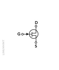 |
N-JFET Transistor | The N-channel junction field effect transistor contains an n-type semiconductive channel that is positioned between the Source (S) and the Drain (D) terminals of the transistor. The Gate (G) arrow which is directed inwards shows the direction of conventional current flow. |
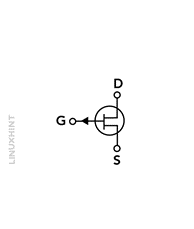 |
P-JFET Transistor | A P-channel junction field effect transistor has a p-type semiconductive channel which is in between the Source (S) and the Drain (D) terminals of the P-JFET transistor. The P-JFET transistor Gate (G) arrow also gives us the direction of current flow. The Gate arrow is pointed outward in the case of a P-JFET transistor. |
 |
N-channel D-MOSFET Transistor | The Depletion N-channel Metal-Oxide-Semiconductor FET (nMOSFET) contains a Gate terminal that is electrically insulated from the primary conductive channel. This transistor is normally in an ON state. It starts conducting when the VG voltages become zero (VG=0). |
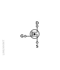 |
P-channel D-MOSFET Transistor | The Depletion P-channel Metal-Oxide-Semiconductor FET (pMOSFET) contains a Gate terminal that is insulated from the primary conductive channel. It is usually in its ON state, and it starts conducting when the VG voltage becomes zero (VG=0). |
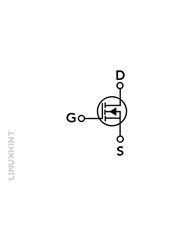 |
N-channel E-MOSFET Transistor | The Enhancement N-channel Metal-Oxide-Semiconductor FET (nMOSFET) contains a Gate terminal that is isolated from the main channel. This transistor is typically in an OFF state and closed when the voltage VG = 0 volts. |
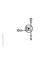 |
P-channel E-MOSFET Transistor | The Enhancement P-channel Metal-Oxide Semiconductor FET (pMOSFET) has a Gate terminal that is separated from the main channel. It is usually in an OFF state and closed when VG = 0 volts. |
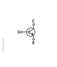 |
IGBT Transistor | An Insulated Gate Bipolar Transistor (IGBT) combines characteristics of both a Bipolar Junction Transistor (BJT) and an Insulated Gate Field Effect Transistor (IGFET). It has high input MOS characteristics and a high bipolar output current-carrying capacity. It also has a low saturation voltage. |
Schematic Semiconductor Symbols for Power Devices
Power semiconductor devices in electrical circuits can convert, regulate, or manage electrical power. These semiconductor devices can handle much higher power levels compared to the bipolar transistors or the field-effect transistors.
Some common power electronics semiconductor devices are Thyristors and Triacs. These devices are driven by the voltage and can be used to switch and control AC power sources. Power semiconductors are used in controlled rectifiers, power supplies, and for AC motor drive controllers.
Power electronics devices are now frequently used in different energy sectors. They have multiple applications in power generation, renewable energy, battery charging systems, power converters, and HVAC.
Some key semiconductor power devices are silicon-controlled rectifiers, gate turn-off rectifiers, triacs, and diacs. Now we will see their schematic symbols and a brief description of each type.
| Schematic Symbol | Symbol Name | Description |
|---|---|---|
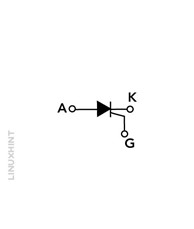 |
Silicon Controlled Rectifier (SCR) | A Silicon Controlled Rectifier (Thyristor) is a 3-terminal semiconductor device. It has a four-layer PNPN structure. SCR has three main terminals: Anode (A), Cathode (K), and Gate (G). Once the Thyristor is triggered, it will continue in its conducting state as long as the current is flowing. Thyristors can also cooperate at higher values of voltages and currents. |
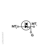 |
Triac | The TRIAC (Triode for Alternating Current) is a 3-terminal device. This bidirectional device can conduct current in both directions. TRIAC has three main terminals named MT2, MT1, and Gate (G). You can easily trigger the TRIAC into conduction mode in any of the directions of the sinusoidal waveform. TRIACs are commonly used in circuits that require bidirectional current control. |
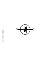 |
Diac | The DIAC (Diode for Alternating Current) is a 2-terminal bidirectional semiconductor device. DIAC is similar to a PNP transistor, but it doesn’t contain a base terminal. It has two diodes which are connected one after the other. To smooth the current conduction process in both directions, you can use the DIACs in combination with the Triac. DIACs are commonly used in AC phase control, speed control, and power control circuits. |
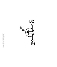 |
Unijunction Transistor (UJT) | The Unijunction Transistor (UJT) is a 3-terminal semiconductor device with a single pn-junction. The main terminals of the UJT are Base-1 (B1), Base-2 (B2), and Emitter (E). Programmable UJTs are also available. You can set their switching parameters using an external resistor. |
Conclusion
Semiconductor schematic symbols are used to represent various semiconductor devices. Using these symbols, we can understand how a semiconductor device works and what a specific symbol represents. These schematic symbols also show us the direction of the current. Using these symbols, we can easily connect any semiconductor device in an electrical circuit by just looking at its schematic symbol.
These schematic symbols of semiconductors use different letter symbols, numbers, and subscripts from the Roman and Greek alphabets. All these are special characters that help us to understand the direction of current input and output. These symbols are not the actual representation of semiconductor devices. The actual device may look different on a circuit board and inside the circuit diagrams.
